A method for reducing the surface defect density of silicon carbide epitaxy
A defect density, silicon carbide technology, applied in the manufacture of electrical components, circuits, semiconductor/solid-state devices, etc., to achieve the effect of reducing surface defect density, simple and easy epitaxy, and uniform in-situ etching
- Summary
- Abstract
- Description
- Claims
- Application Information
AI Technical Summary
Problems solved by technology
Method used
Image
Examples
Embodiment Construction
[0023] The technical solutions of the present invention will be further described below in conjunction with the accompanying drawings and embodiments.
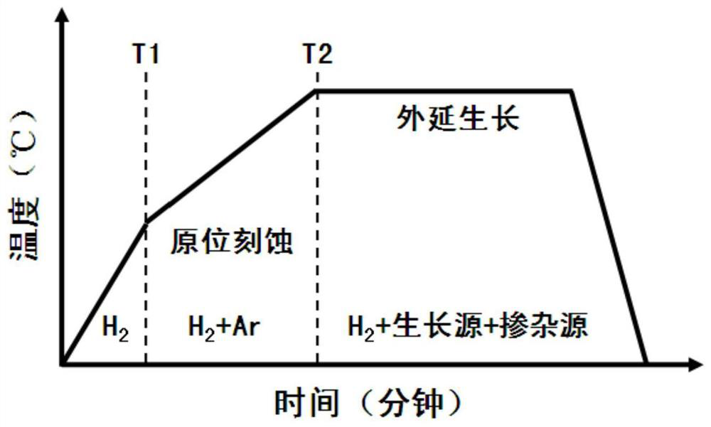
[0024] Such as figure 1 As shown, the method for reducing the surface defect density of silicon carbide epitaxy described in the present invention comprises steps:
[0025] (1) Place the cleaned SiC substrate on the pedestal in the chemical vapor deposition (CVD) equipment. The silicon carbide substrate can be a 3-8 inch silicon carbide substrate that is 4° to the direction;
[0026] (2) set reaction chamber pressure to be 80-150mbar, hydrogen (H 2 ) The flow rate is 80-150L / min, and the system heats up to a temperature of 1400-1500°C;
[0027] (3) Keep the temperature and reaction chamber pressure constant, and perform pure hydrogen etching on the substrate for 1-10 minutes;
[0028] (4) Keep the pressure and H 2 The flow rate is constant, and a small flow rate of argon (Ar) is introduced into the reaction chamber to ass...
PUM
 Abstract
Description
Claims
Application Information
 - Generate Ideas
- Intellectual Property
- Life Sciences
- Materials
- Tech Scout
- Unparalleled Data Quality
- Higher Quality Content
- 60% Fewer Hallucinations
Browse by: Latest US Patents, China's latest patents, Technical Efficacy Thesaurus, Application Domain, Technology Topic, Popular Technical Reports.
© 2025 PatSnap. All rights reserved.Legal|Privacy policy|Modern Slavery Act Transparency Statement|Sitemap|About US| Contact US: help@patsnap.com


