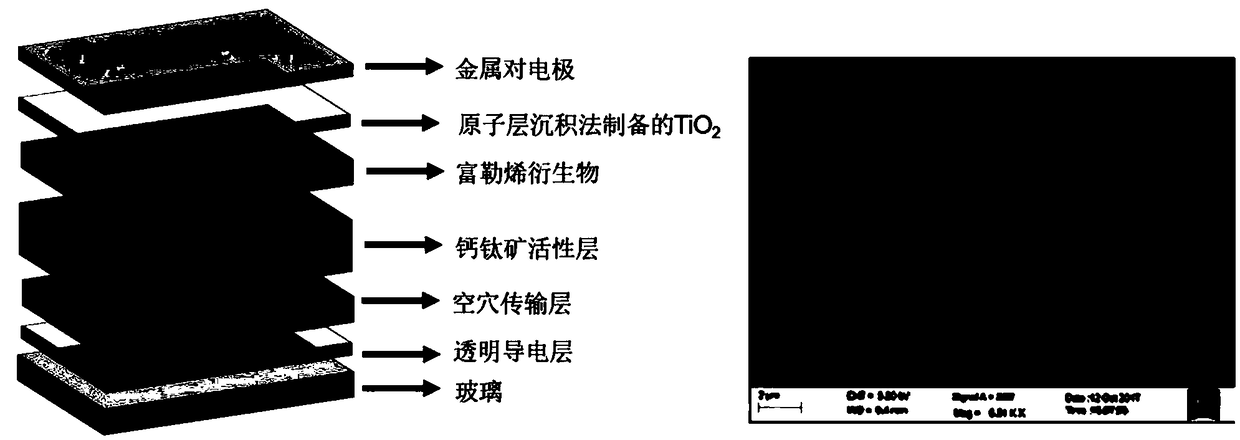
Composite electron transfer layer perovskite solar cell prepared by using atomic layer deposition method and preparation method thereof
A technology of atomic layer deposition and electron transport layer, which is applied in circuits, photovoltaic power generation, electrical components, etc., can solve the problems of inability to effectively block the diffusion of perovskite components and top electrodes, and the destruction of perovskite active layers
- Summary
- Abstract
- Description
- Claims
- Application Information
AI Technical Summary
Problems solved by technology
Method used
Image
Examples
Embodiment 1
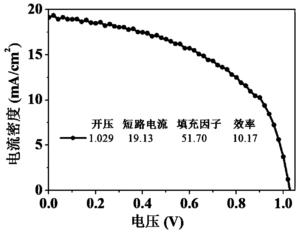
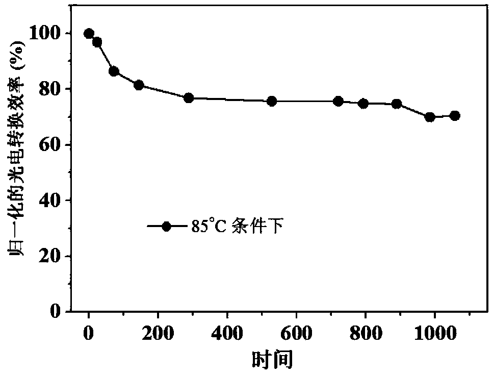
[0023] The transparent conductive substrate FTO was cleaned with acetone, ethanol, and isopropanol, and a 2.0% by mass ethanol solution of nickel acetate was coated to form a film by spin coating, and annealed at 400° C. for 30 minutes. Weigh 550mg PbI 2 , 20mg CsI, dissolved it in 1mL DMF solvent, and prepared 3mL isopropanol iodoformamidine solution. On the NiO substrate, PbI was first prepared by spin coating 2 The thin film was annealed at 70°C for 10min, and then the isopropanol solution of iodoformidin was spin-coated on PbI 2 On the thin film, the perovskite photoactive layer can be prepared after annealing at 160 °C for 15 min. A solution of a fullerene derivative in a non-polar solvent is first coated on the perovskite layer. Using the atomic layer deposition system, under the condition of the substrate temperature of 100 ℃, using TiCl 4 and water as the precursor to deposit a layer of TiO with a thickness of about 50 nm after multiple cycles 2 layer, and placed ...
Embodiment 2
[0026] The transparent conductive substrate FTO was cleaned with acetone, ethanol, and isopropanol, and a 2.0% by mass ethanol solution of nickel acetate was coated to form a film by spin coating, and annealed at 400° C. for 30 minutes. Weigh 550mg PbI 2 , 20mg CsI, dissolved it in 1mL DMF solvent, and prepared 3mL isopropanol iodoformamidine solution. On the NiO substrate, PbI was first prepared by spin coating 2 The thin film was annealed at 70°C for 10min, and then the isopropanol solution of iodoformidin was spin-coated on PbI 2 On the thin film, the perovskite photoactive layer can be prepared after annealing at 160 °C for 15 min. A solution of a fullerene derivative in a non-polar solvent is first coated on the perovskite layer. Using the atomic layer deposition system, under the condition of the substrate temperature of 100 ℃, using TiCl 4 and water as the precursor to deposit a layer of TiO with a thickness of about 50 nm after multiple cycles 2 layer, under high ...
Embodiment 3
[0029] The transparent conductive substrate FTO was cleaned with acetone, ethanol, and isopropanol, and a 2.0% by mass ethanol solution of nickel acetate was coated to form a film by spin coating, and annealed at 400° C. for 30 minutes. Weigh 550mg PbI 2 , 20mg CsI, dissolved it in 1mL DMF solvent, and prepared 3mL isopropanol iodoformamidine solution. On the NiO substrate, PbI was first prepared by spin coating 2 The thin film was annealed at 70°C for 10min, and then the isopropanol solution of iodoformidin was spin-coated on PbI 2 On the thin film, the perovskite photoactive layer can be prepared after annealing at 160 °C for 15 min. A solution of a fullerene derivative in a non-polar solvent is first coated on the perovskite layer. Using the atomic layer deposition system, under the condition of the substrate temperature of 100 ℃, using TiCl 4 and water as the precursor to deposit a layer of TiO with a thickness of about 50 nm after multiple cycles 2 layer, under high ...
PUM
| Property | Measurement | Unit |
|---|---|---|
| Thickness | aaaaa | aaaaa |
Abstract
Description
Claims
Application Information
 - R&D
- Intellectual Property
- Life Sciences
- Materials
- Tech Scout
- Unparalleled Data Quality
- Higher Quality Content
- 60% Fewer Hallucinations
Browse by: Latest US Patents, China's latest patents, Technical Efficacy Thesaurus, Application Domain, Technology Topic, Popular Technical Reports.
© 2025 PatSnap. All rights reserved.Legal|Privacy policy|Modern Slavery Act Transparency Statement|Sitemap|About US| Contact US: help@patsnap.com


