Self-aligned silicon germanium hbt device monitors the structure and process method of silicon germanium base region doping

A process method and self-alignment technology, applied in the manufacture of semiconductor devices, electrical solid-state devices, semiconductor/solid-state devices, etc., can solve the problems of load effect, high cost, SIMS cannot reflect the distribution of device impurities, etc., and achieve easy implementation, The effect of simple implementation

Active Publication Date: 2022-03-08
SHANGHAI HUAHONG GRACE SEMICON MFG CORP
View PDF4 Cites 0 Cited by
  • Summary
  • Abstract
  • Description
  • Claims
  • Application Information

AI Technical Summary

Problems solved by technology

[0005] Since the impurity distribution of the HBT vertical device, especially the impurity distribution in the base region, has a great influence on the DC and RF characteristics, it is generally characterized by secondary ion mass spectrometry (SIMS) in the development process; however, the SIMS method has a long cycle and high cost, and Epitaxial growth has a load effect, and the thickness of silicon germanium grown in the larger active region is larger than that of the smaller active region, while the active region of the SIMS structure is larger and the active region of the device is smaller, and the SIMS morphology cannot reflect Impurity distribution in the device

Method used


Image

  • Self-aligned silicon germanium hbt device monitors the structure and process method of silicon germanium base region doping
  • Self-aligned silicon germanium hbt device monitors the structure and process method of silicon germanium base region doping
  • Self-aligned silicon germanium hbt device monitors the structure and process method of silicon germanium base region doping

Examples


Embodiment Construction

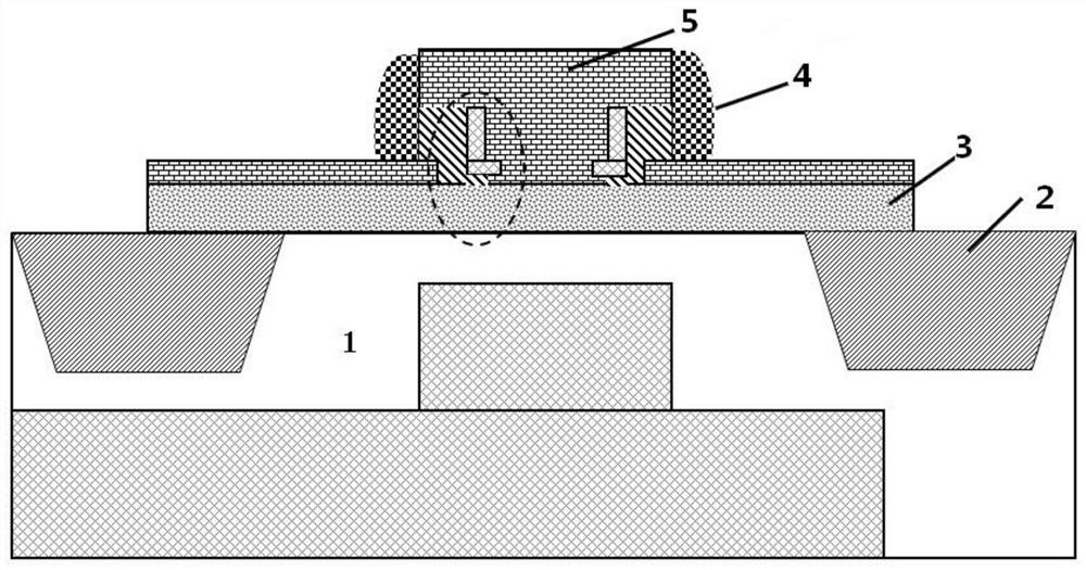
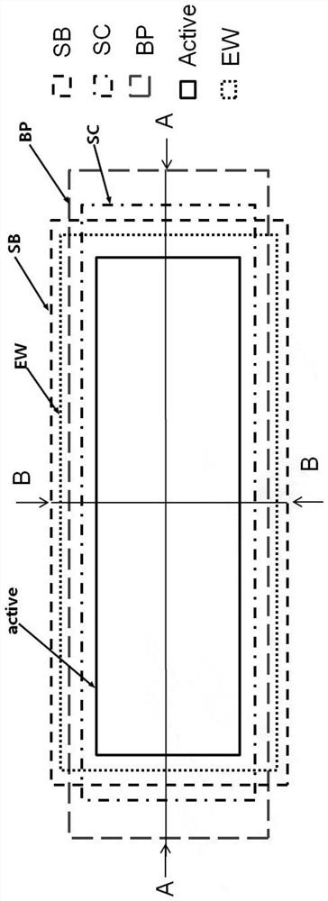
[0046] The self-aligned silicon germanium HBT device of the present invention monitors the test structure of the silicon germanium epitaxial layer doping, the layout of the test structure is as follows figure 2 shown, including:

[0047]The active area is a rectangle, and a rectangular etch-back protective layer SC, base polysilicon BP, sacrificial emitter window EW, and metal silicide barrier layer SB located outside the active area and surrounding the active area layer by layer ; Each of the layers is axially symmetrical with respect to the length and width of the active region.

[0048] In the length direction of the active region, that is, the AA direction from the inside to the outside, there are sacrificial emitter window EW, metal silicide barrier layer SB, etch-back protective layer SC and the boundary BP of the base polysilicon.

[0049] In the width direction of the active region, that is, the BB direction from the inside to the outside is the boundary of the etch-...


PUM

PropertyMeasurementUnit
thicknessaaaaaaaaaa
thicknessaaaaaaaaaa
thicknessaaaaaaaaaa

Abstract

The invention discloses a self-aligned silicon-germanium HBT device to monitor the doping test structure of the germanium-silicon base area after the diffusion of the emission area, which comprises: a rectangular active area, and a layer-by-layer active area located outside the active area. The surrounding rectangular etch-back protection area, base polysilicon, sacrificial emitter window and metal silicide barrier layer; in the length direction of the active region, from the inside to the outside are sacrificial emitter window, metal silicide barrier layer, The boundary of the etch-back protection area and the polysilicon in the base area; in the width direction of the active area, from the inside to the outside are the boundaries of the etch-back protection area, the base area polysilicon, the sacrificial emitter window and the metal silicide barrier layer. The invention can effectively monitor the P-type doping concentration of the epitaxial layer in the self-aligned silicon-germanium HBT device in the electrical test stage of the silicon wafer, can compare the P-type concentration of different menus in the research and development process, and can monitor the silicon-germanium in the mass production process Epitaxy process stability. The process method described in the invention is compatible with the original process, and is simple and easy to implement.

Description

technical field [0001] The present invention relates to the field of design and manufacture of semiconductor devices, in particular to a test structure that adopts a non-selective epitaxial self-aligned silicon-germanium HBT device to monitor the doping of the epitaxially grown silicon-germanium base region. The present invention also relates to the structure process method. Background technique [0002] P-type polysilicon is used to raise the outer base region, and a self-aligned device structure with inner walls is used between the emitter and the outer base region, such as figure 1 , can reduce the base resistance and base-collector capacitance at the same time, such silicon germanium HBT devices can obtain the highest oscillation frequency fmax greater than 300GHz, and its performance can be comparable to III-V semiconductor devices, and is widely used in optical communication and mmWave applications. [0003] SiGe HBT devices use germanium-silicon-carbon alloy doped w...

Claims


Application Information

Patent Timeline
Patent Type & Authority Patents(China)
IPC IPC(8): H01L21/331H01L23/544H01L21/66
CPCH01L23/544H01L29/66318H01L22/30
Inventor 周正良
Owner SHANGHAI HUAHONG GRACE SEMICON MFG CORP
Why Eureka
Try Eureka