
Patsnap Eureka
For R&D, Patsnap Eureka makes reading and utilizing patents & technical documents easy.
Patsnap Eureka AIR
Designed for self-driven R&D workflows. Generate viable solutions, solve complex R&D challenges, empower your innovation with AI.

Patsnap Eureka Materials
Designed for material experts only. Revolutionize your material R&D, from search, analyze, to developing new materials.

TechResearch
Generate reliable direction feasibility study reports for your R&D in just a few steps.

TechSeek
Discover and master advanced knowledge NOW. Basics, ideas, possibilities, all at once.

TechMind
As an expert in R&D Theories, TechMind can generates customized viable solutions instantly.

TechRisk
Analyze your overall solution with one click, know your potential R&D risks in advance.

TechMonitor
Get weekly tech updates, stay abreast of the latest tech innovations and key insights.
Monitoring wafer and monitoring system
A monitoring system and wafer technology, applied in electrical components, semiconductor/solid-state device manufacturing, circuits, etc., can solve problems such as pollution and low maintenance efficiency, and achieve the effect of ensuring accuracy
- Summary
- Abstract
- Description
- Claims
- Application Information
AI Technical Summary
Problems solved by technology
Method used
Image

Examples
Embodiment Construction
[0024] In order to make the purpose, technical solutions and advantages of the embodiments of the present invention clearer, the embodiments of the present invention will be described in detail below with reference to the accompanying drawings. However, those skilled in the art can understand that in each embodiment of the present invention, many technical details are provided for readers to better understand the present application. However, even without these technical details and various changes and modifications based on the following embodiments, the technical solutions claimed in this application can also be realized.
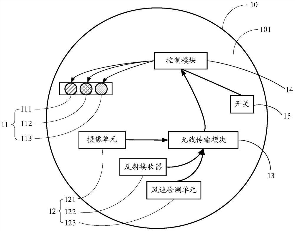
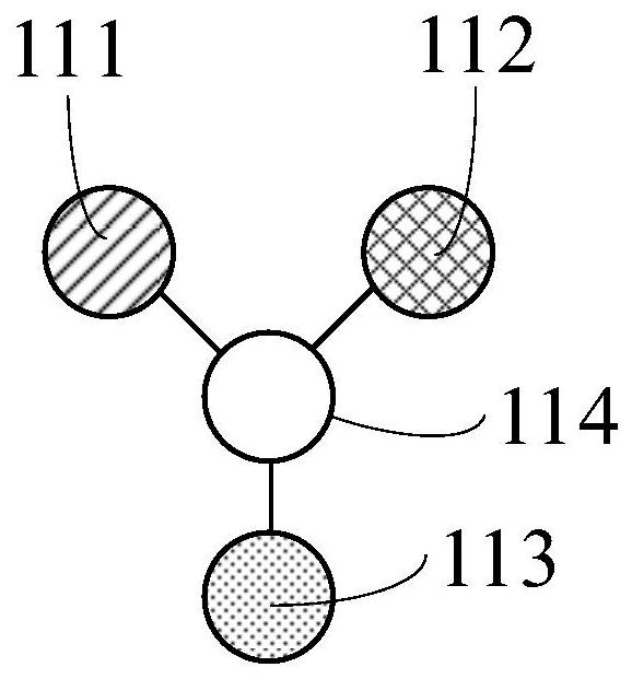
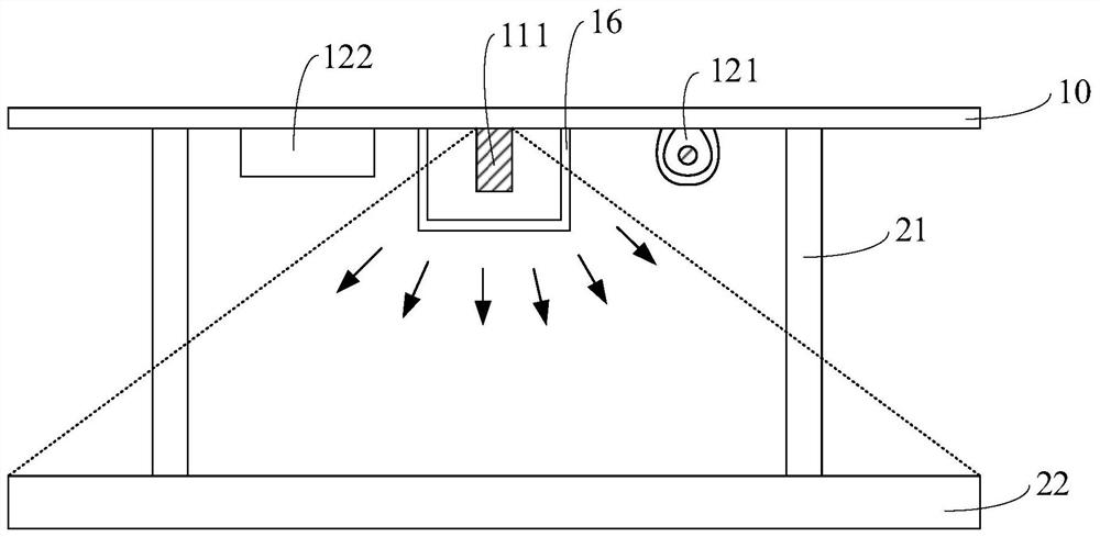
[0025] refer to figure 1 , the monitoring wafer comprises: initial wafer 10, initial wafer 10 has front and back 101, and back 101 faces wafer chuck (not shown); Wireless transmission module 13 and the camera module 11 and data acquisition that are positioned at back 101 Module 12, the search module 11 is used to send search light to the wafer chuck, the...
PUM
 Abstract
Description
Claims
Application Information
 - R&D Engineer
- R&D Manager
- IP Professional
- Industry Leading Data Capabilities
- Powerful AI technology
- Patent DNA Extraction
Browse by: Latest US Patents, China's latest patents, Technical Efficacy Thesaurus, Application Domain, Technology Topic, Popular Technical Reports.
© 2024 PatSnap. All rights reserved.Legal|Privacy policy|Modern Slavery Act Transparency Statement|Sitemap|About US| Contact US: help@patsnap.com