Self-aligned silicon germanium hbt device monitors the structure and process method of intrinsic base doping

A technology of intrinsic base area and process method, which is applied in the direction of semiconductor devices, semiconductor/solid-state device manufacturing, electrical components, etc., can solve the problems of small devices, high cost, and inability to reflect the distribution of device impurities, and achieve easy implementation and simple implementation Effect

Active Publication Date: 2022-05-20
SHANGHAI HUAHONG GRACE SEMICON MFG CORP
View PDF0 Cites 0 Cited by
  • Summary
  • Abstract
  • Description
  • Claims
  • Application Information

AI Technical Summary

Problems solved by technology

[0006] However, the SIMS method has a long period and high cost, and the epitaxial growth has a load effect. The thickness of the silicon germanium grown in the larger active region is larger than that of the smaller active region, while the active region of the SIMS structure is larger and the active region of the device is larger. The area is small, and the morphology of SIMS cannot reflect the distribution of impurities in the device

Method used


Image

  • Self-aligned silicon germanium hbt device monitors the structure and process method of intrinsic base doping
  • Self-aligned silicon germanium hbt device monitors the structure and process method of intrinsic base doping
  • Self-aligned silicon germanium hbt device monitors the structure and process method of intrinsic base doping

Examples


Embodiment Construction

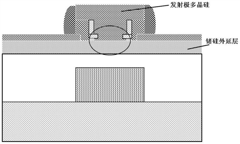
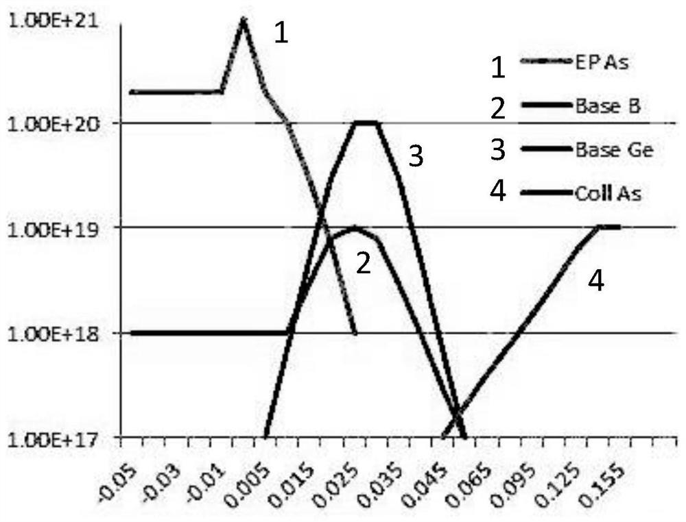
[0048] The self-aligned silicon-germanium HBT device described in the present invention monitors the test structure of the silicon-germanium base region doped after the emission region is diffused, and the layout of the test structure is as follows image 3 As shown, in the length direction, it is composed of two parts in series: one part is composed of high-doped resistance in the outer base region and the link resistance in series, and the other part is the pinch resistance after the emitter region diffuses to the base region.

[0049] It is also composed of two parts in the width direction: there are undoped silicon germanium epitaxial region resistors on both sides, and these two resistors are connected in parallel.

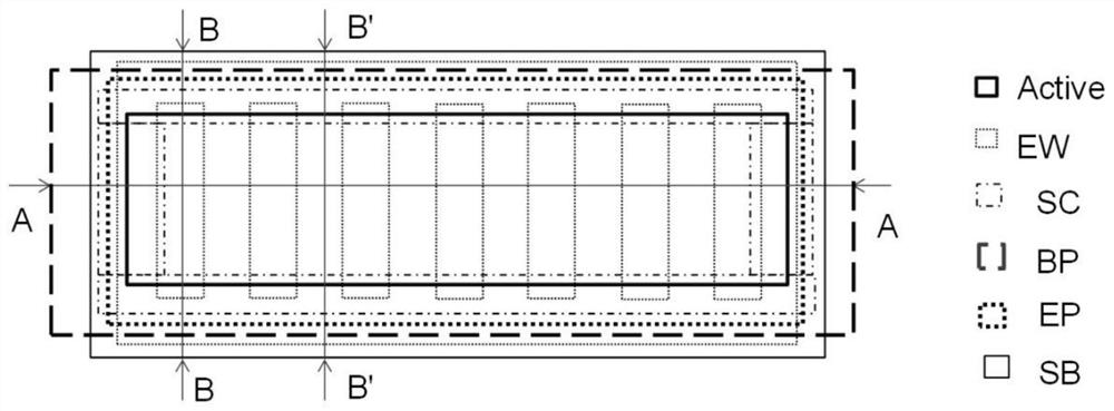
[0050] On the rectangular active area, there are multiple rectangular sacrificial emitter windows vertically overlapping with the active area, which exceed the width of the active area in the length direction, and the etch-back protection area covers all the a...


PUM

PropertyMeasurementUnit
thicknessaaaaaaaaaa
thicknessaaaaaaaaaa

Abstract

The invention discloses a test structure for monitoring the doping of the intrinsic base region (the germanium-silicon base region after diffusion of the emitter region) of a self-aligned silicon-germanium HBT device. The test structure is composed of two parts connected in series in the length direction. : One part is composed of the high-doped silicon germanium region resistance in the outer base region and the link resistance in the undoped silicon germanium epitaxial region in series, and the other part is the pinch resistance after the emitter region diffuses to the base region; it also consists of two parts in the width direction Composition: There are undoped silicon germanium epitaxial region link resistors on both sides, and the series resistor in the middle; these two resistors are connected in parallel. The invention can effectively monitor the doping concentration of the intrinsic base region in the self-aligned silicon-germanium HBT device, and can compare the P-type concentration of different silicon-germanium process menus in the research and development process, as well as the influence of emitter doping and thermal overhead, and Compared with the electrical test results of HBT devices to verify whether the experiment meets the design requirements; in the mass production process, the process stability of silicon germanium epitaxy and emitter doping and thermal overhead can be monitored.

Description

technical field [0001] The present invention relates to the field of design and manufacture of semiconductor devices, in particular to a self-aligned silicon-germanium HBT device using non-selective epitaxy to monitor the doping concentration of the intrinsic base region (germanium-silicon base region after diffusion of the emitter region). The invention also discloses a process method of the structure. Background technique [0002] P-type polysilicon is used to raise the outer base region, and a self-aligned device structure with inner walls is used between the emitter and the outer base region, such as figure 1 As shown, the base resistance and the base-collector capacitance can be reduced at the same time. Such a silicon germanium HBT device can obtain the highest oscillation frequency fmax greater than 300 GHz, and its performance can be comparable to that of III-V compound semiconductor devices. It is widely used in Optical communications and mmWave applications. [0...

Claims


Application Information

Patent Timeline
Patent Type & Authority Patents(China)
IPC IPC(8): H01L29/778H01L21/335H01L29/06
CPCH01L29/0603H01L29/0684H01L29/66462H01L29/778
Inventor 周正良
Owner SHANGHAI HUAHONG GRACE SEMICON MFG CORP
Why Eureka
Try Eureka