Tunneling field effect transistor and method of making the same

A tunneling field effect and transistor technology, which is applied in semiconductor/solid-state device manufacturing, diodes, semiconductor devices, etc., can solve the problems of small tunneling current and large tunneling barrier resistance of tunneling field effect transistors

Active Publication Date: 2020-10-16
HUAWEI TECH CO LTD
View PDF9 Cites 0 Cited by
  • Summary
  • Abstract
  • Description
  • Claims
  • Application Information

AI Technical Summary

Problems solved by technology

[0004] However, due to the large tunneling barrier resistance of the tunneling field effect transistor, the tunneling current of the tunneling field effect transistor is small

Method used


Image

  • Tunneling field effect transistor and method of making the same
  • Tunneling field effect transistor and method of making the same
  • Tunneling field effect transistor and method of making the same

Examples


Embodiment Construction

[0102] In order to make the purpose, technical solution and advantages of the present application clearer, the implementation manners of the present application will be further described in detail below in conjunction with the accompanying drawings.

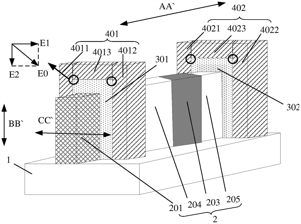
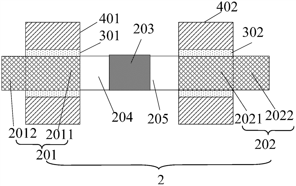
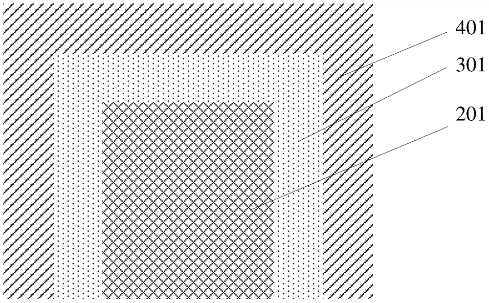
[0103] The embodiment of the present application provides a tunneling field effect transistor, which is now combined with figure 1 and figure 2 In detail, among them, figure 1 is a schematic diagram of the three-dimensional structure of the tunneling field effect transistor, figure 2 for will figure 1 The cross-sectional view of the tunneling field effect transistor shown along CC' cutting. see figure 1 , the tunneling field effect transistor includes: a substrate layer 1;

[0104] A rectangular semiconductor strip 2 formed on the upper surface of the substrate layer 1, the rectangular semiconductor strip 2 is sequentially provided with a first source region 201, a first channel region 204, a drain region 203, a second cha...


PUM


Abstract

A tunneling field effect transistor and a method for preparing the same, comprising: a substrate layer (1); a rectangular semiconductor strip (2) formed on an upper surface of the substrate layer, the rectangular semiconductor strip being sequentially provided with first source regions (201 along a first direction) ), a first channel region (204), a drain region (203), a second channel region (205) and a second source region (202); covering the first portion (2011) and the second source region of the first source region The first gate dielectric layer (301) and the second gate dielectric layer (302) on the outer surface of the third part (2021) of the region; the first gate region (401) covering the outer surface of the first gate dielectric layer, the first gate The direction of the electric field applied to the region points to the first source region; the second gate region (402) covering the outer surface of the second gate dielectric layer, the direction of the electric field applied to the second gate region points to the second source region. The design of dual source regions increases the tunneling area of ​​carriers in the source region, and the direction of the electric field applied in the gate region is consistent with the tunneling direction of carriers in the source region, which increases the tunneling probability. The penetration area is proportional to the tunneling probability, so the tunneling current is larger.

Description

technical field [0001] The present application relates to the field of semiconductor technology, in particular to a tunneling field effect transistor and a preparation method thereof. Background technique [0002] With the continuous development of semiconductor technology, the size of MOSFET (Metal Oxide Semiconductor Field Effect Transistor, Metal Oxide Semiconductor Field Effect Transistor) continues to shrink according to Moore's Law. However, limited by the Boltzmann distribution of carriers at room temperature, the subthreshold swing SS of the MOSFET cannot be reduced synchronously with the shrinking of the device size, and is always greater than 60mV / decade, which makes it possible for small-sized devices to MOSFET consumes a lot of power. In order to meet the development requirements of high-density, high-performance, and low-cost semiconductors, tunneling field effect transistors (English: Tunnel Field Effect Transsistor, TFET for short) are applied. [0003] The ...

Claims


Application Information

Patent Timeline
IPC IPC(8): H01L29/78
CPCH01L29/7391H01L29/66356H01L29/42312H01L29/0657B82Y10/00H01L27/06H01L29/78H01L21/3086H01L29/0847H01L29/1033H01L29/66484H01L29/66977
Inventor 赵静张臣雄
Owner HUAWEI TECH CO LTD
Why Eureka
Try Eureka