Semiconductor device and method of forming the same

A semiconductor and device technology, applied in the field of semiconductor devices and their formation, can solve problems such as poor performance of semiconductor devices, and achieve the effect of improving the current crowding effect

Active Publication Date: 2021-03-09
SEMICON MFG INT (SHANGHAI) CORP +1
View PDF6 Cites 0 Cited by
  • Summary
  • Abstract
  • Description
  • Claims
  • Application Information

AI Technical Summary

Problems solved by technology

[0004] However, the performance of semiconductor devices formed by prior art is poor

Method used


Image

  • Semiconductor device and method of forming the same
  • Semiconductor device and method of forming the same
  • Semiconductor device and method of forming the same

Examples


Embodiment Construction

[0032] As mentioned in the background, semiconductor devices formed in the prior art have poor performance.

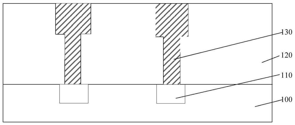
[0033] figure 1 It is a schematic structural diagram of a semiconductor device, and the semiconductor device includes: a substrate 100 with an underlying metal layer 110 inside; a dielectric layer 120 located on the substrate 100; an interconnection layer opening penetrating through the dielectric layer 120, the The underlying metal layer 110 is exposed through the opening of the interconnection layer, and the opening of the interconnection layer includes a contact hole and a trench on the contact hole; the conductive layer 130 is located in the opening of the interconnection layer.

[0034] However, the electrical performance of the above-mentioned semiconductor devices is poor, and it is found through research that the reasons are:

[0035] The conductive layer 130 in the contact hole is used to electrically connect the underlying metal layer 110 with the conductive...


PUM

PropertyMeasurementUnit
relative permittivityaaaaaaaaaa

Abstract

A semiconductor device and a method for forming the same, wherein the method includes: providing a substrate and a dielectric layer on the substrate, wherein the substrate has an underlying metal layer; forming an interconnection layer opening through the dielectric layer in the dielectric layer, the interconnection The layer opening exposes the bottom metal layer, and the interconnection layer opening includes a contact hole and a trench on the contact hole; a first conductive layer is formed in the contact hole, from the bottom metal layer to the direction of the top surface of the first conductive layer Above, the material of the first conductive layer has a first conductivity; after forming the first conductive layer, a second conductive layer is formed in the trench, and in a direction parallel to the top surface of the substrate, the material of the second conductive layer has The second conductivity, the first conductivity is greater than the second conductivity. The method improves the electrical performance of the semiconductor device.

Description

technical field [0001] The invention relates to the field of semiconductor manufacturing, in particular to a semiconductor device and a forming method thereof. Background technique [0002] With the continuous advancement of semiconductor integrated circuit process technology, when semiconductor devices are reduced to a deep submicron range, high-performance, high-density connections between semiconductor devices need to be realized through interconnect structures. It is easy to form parasitic resistance and parasitic capacitance in the interconnection structure, resulting in parasitic effect, which leads to the time delay of metal connection transmission. People are faced with how to overcome the RC caused by the rapid growth of connection length (R refers to resistance, C refers to capacitance) A problem with significantly increased latency. [0003] In order to overcome the parasitic effect in the interconnection, in the integrated process of the back-end process interco...

Claims


Application Information

Patent Timeline
Patent Type & Authority Patents(China)
IPC IPC(8): H01L21/768H01L23/522H01L23/532
CPCH01L21/76877H01L23/5226H01L23/53204H01L23/53276H01L21/76811H01L21/76813H01L21/76876H01L2221/1094H01L21/28556H01L21/31116H01L21/31144H01L21/3212H01L21/32135H01L21/76802H01L21/7684H01L21/76846H01L21/76879H01L23/528H01L23/53238H01L2221/1089
Inventor 张海洋张城龙蒋鑫
Owner SEMICON MFG INT (SHANGHAI) CORP
Why Eureka
Try Eureka