
Standard cell library design method, design device, standard cell library and CMOS image sensing chip

A standard cell library and design method technology, applied in the field of image processing, can solve problems such as speed and accuracy loss, and achieve the effects of improving stability, reducing speed and accuracy loss, and reducing economic costs.

Active Publication Date: 2018-10-12
SHENZHEN UNIV
View PDF6 Cites 12 Cited by
  • Summary
  • Abstract
  • Description
  • Claims
  • Application Information

AI Technical Summary

Problems solved by technology

This makes if the standard cell library of the digital logic process is used when designing the peripheral circuit of the CMOS image sensor chip, the level conversion unit circuit is required to realize the docking with the core circuit of the CMOS image sensor chip, so that the design has speed and loss of precision

Method used


Image

  • Standard cell library design method, design device, standard cell library and CMOS image sensing chip
  • Standard cell library design method, design device, standard cell library and CMOS image sensing chip
  • Standard cell library design method, design device, standard cell library and CMOS image sensing chip

Examples


Embodiment Construction

[0029]The present invention will be further described below with reference to the accompanying drawings and exemplary embodiments, examples of which are shown in the accompanying drawings, wherein the same or similar reference numerals represent the same or similar elements or elements with the same or similar functions . The embodiments described below by referring to the figures are exemplary only for explaining the present invention and should not be construed as limiting the present invention. Also, detailed descriptions of known arts will be omitted if they are unnecessary to illustrate the features of the present invention.

[0030] Those skilled in the art will understand that unless otherwise stated, the singular forms "a", "an", "said" and "the" used herein may also include plural forms. It should be further understood that the word "comprising" used in the description of the present invention refers to the presence of said features, integers, steps, operations, elem...


PUM


Abstract

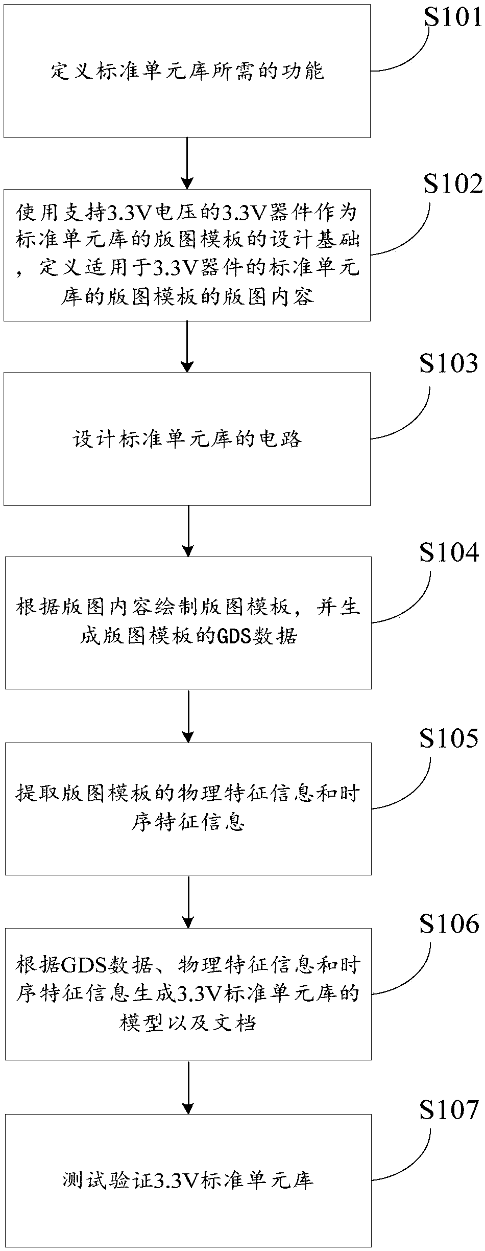
The invention provides a standard cell library design method, a design device, a standard cell library and a CMOS image sensing chip. The method comprises the steps that the functions of the standardcell library are defined; a 3.3V device supporting 3.3V voltage is used as a design basis of a layout template of the standard cell library, and layout content suitable for the layout template of thestandard cell library of the 3.3V device is defined; a circuit of the standard cell library is designed; the layout template is drawn according to the layout content; physical feature information andtime sequence feature information of the layout template are extracted; according to GDS data, the physical feature information and the time sequence feature information, a model and a document of thestandard cell library are generated; and the standard cell library is verified through a test. Through the method, communication between a peripheral circuit and a core circuit of the CMOS image sensing chip based on digital logic process design can be realized, speed and precision losses brought by a level switching circuit are reduced, and system speed and performance stability are improved.

Description

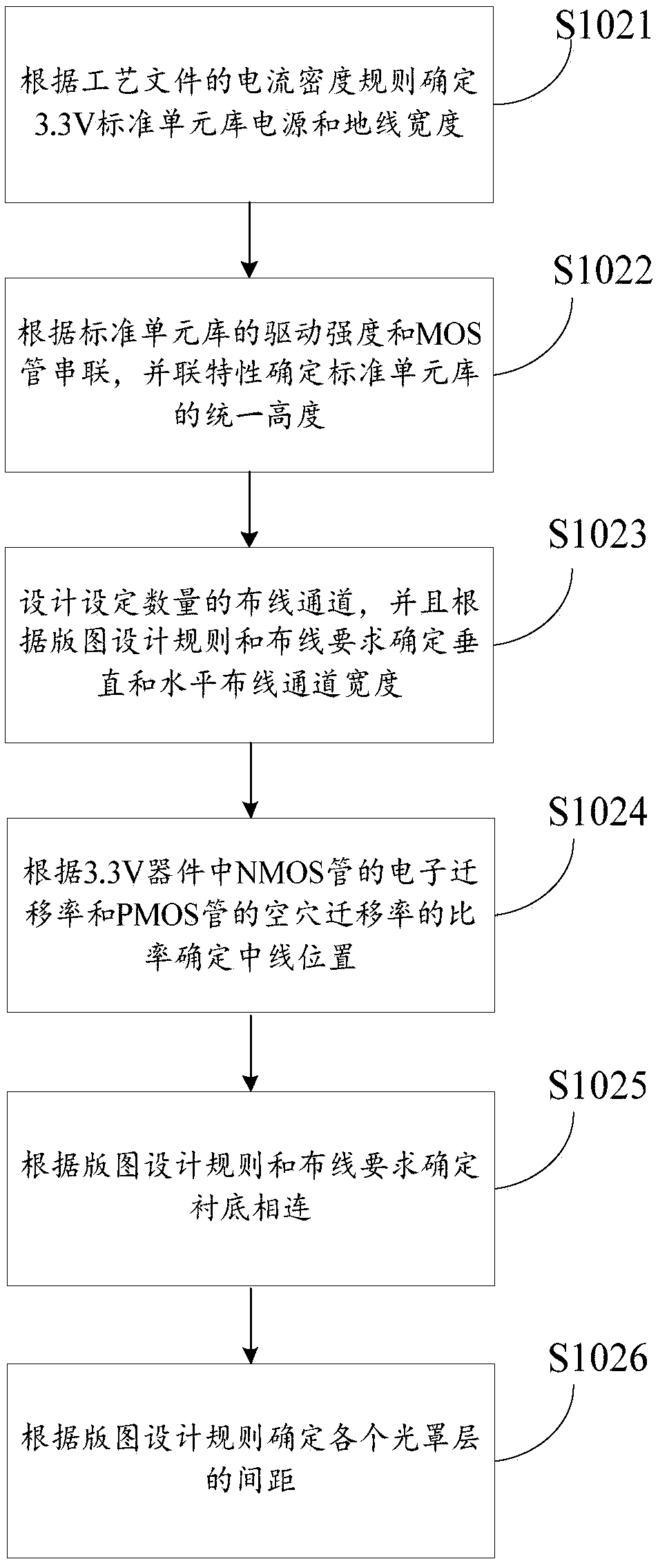
technical field [0001] The application relates to the field of image processing, in particular to a standard cell library design method, a design device, a standard cell library and a CMOS image sensor chip. Background technique [0002] With the rapid development of Moore's Law, integrated circuits have entered the nanometer process node, and the integration and complexity of chips are increasing. The semi-custom chip design method based on the standard cell library has been widely used in the design of ultra-large-scale digital chips. The standard cell library is a general term for the unit symbol library, circuit structure library, function description library, layout library, timing power library, physical view library, design rules and interconnection parasitic parameter model library required for integrated circuit design. [0003] The standard cell library is the basis of integrated circuit design. From system behavior description, logic synthesis, logic function simu...

Claims


Application Information

Patent Timeline
Patent Type & Authority Applications(China)
IPC IPC(8): G06F17/50
CPCG06F30/398G06F30/392
Inventor 徐渊黄志宇谢刚张楷彬杨俊伟廖嘉雯
Owner SHENZHEN UNIV
Learn More