Downlink level shifting circuit with low operating voltage

A technology of level shifting circuit and working voltage, which is applied in the direction of logic circuit interface device, logic circuit connection/interface layout, etc., can solve the problems of MN3 and MN4 not working normally, low gate voltage, and circuit not working normally, etc., to achieve Broaden the operating voltage range, wide application range, and improve the effect of grid voltage

Pending Publication Date: 2018-10-02
无锡安趋电子有限公司
View PDF0 Cites 10 Cited by
  • Summary
  • Abstract
  • Description
  • Claims
  • Application Information

AI Technical Summary

Problems solved by technology

Correspondingly, although this structure solves the withstand voltage problem between the high-side and low-side levels, when the voltage between the high-side high-level VB and the high-side low-level VS in the high-voltage region is low, it will make the NMOS transistor MN3 1. The gate voltage of MN4 is low, and MN3 and MN4 cannot work normally, resulting in the failure of the entire circuit to work normally.

Method used


Image

  • Downlink level shifting circuit with low operating voltage
  • Downlink level shifting circuit with low operating voltage
  • Downlink level shifting circuit with low operating voltage

Examples


Embodiment Construction

[0032] The principles and features of the present invention will be described below in conjunction with the accompanying drawings, and the examples given are only used to explain the present invention, and are not intended to limit the scope of the present invention.

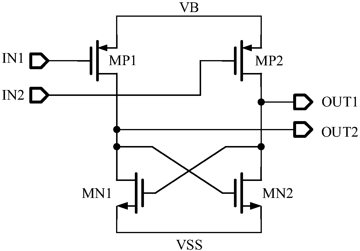
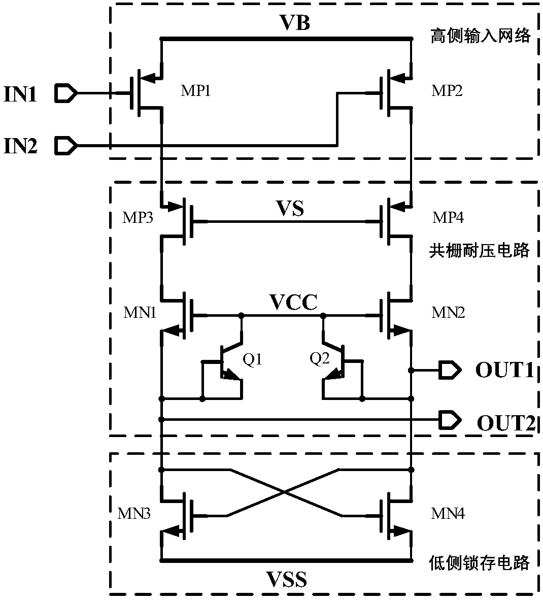
[0033] Such as Figure 4 , is a circuit diagram of the downlink level shift circuit for reducing the minimum operating voltage of the present invention, including three parts, namely, a high-side input network, a common-gate withstand voltage circuit and a low-side latch circuit.

[0034] The working level of the high-side input network is between VB and VS. In the high-voltage area, the high-level VB on the high-side is equivalent to the high-side "power supply", and the high-side low-level VS is equivalent to the high-side "ground". The high-side input network is used to transfer the input signal IN to the next-level circuit. It adopts a dual-input and dual-output PMOS common-source circuit. The two-way PMOS c...


PUM


Abstract

A downlink level shifting circuit includes a high side input network, a common gate voltage-withstanding structure and a low side latch circuit; the high side input network consists of two parallel PMOS devices of a common source structure, and transmits an input signal to the common gate voltage-withstanding structure; the common gate voltage-withstanding circuit includes a pair of common gate PMOS transistors, a pair of common gate NMOS transistors and two clamp diodes; and the low side latch circuit includes two pairs of NMOS transistors used as linear resistors and a latch structure formedby a pair of cross-coupled NMOS devices, and enables a high-side signal to be transmitted to a low-voltage region when a high-side voltage difference is very small.

Description

technical field [0001] The present invention relates to a level shift circuit in the field of half-bridge drive technology, in particular to a low working voltage downlink level shift circuit that converts a high-voltage level signal into a low-voltage level signal Background technique [0002] With the rapid development of electronic power technology, especially the increasingly wide application of high-frequency self-turn-off components such as IGBT and MOSFET, the design of the drive circuit is very important, especially the high-voltage integrated circuit HVIC drive. A good driving circuit can ensure the high-performance operation of the HVIC chip, such as excellent system reliability and efficiency. In current consumer and industrial applications, HVICs are widely used in many fields, such as variable frequency motor drives, switching power supplies, and electronic ballasts. [0003] figure 1 is the internal block diagram of a traditional HVIC drive circuit. A tradit...

Claims


Application Information

Patent Timeline
Patent Type & Authority Applications(China)
IPC IPC(8): H03K19/0175
CPCH03K19/017509
Inventor 张允武方子木余思远
Owner 无锡安趋电子有限公司
Why Eureka
Try Eureka