GaN device based on component-gradient GaN MISFET and preparing method thereof

A component and device technology, applied in the field of microelectronics, can solve the problems that restrict the improvement of device performance, high surface states and defects, and poor device withstand voltage characteristics, so as to achieve the goal of increasing power density, reducing leakage current, and reducing state density Effect

Inactive Publication Date: 2009-07-08
XIDIAN UNIV
View PDF5 Cites 0 Cited by
  • Summary
  • Abstract
  • Description
  • Claims
  • Application Information

AI Technical Summary

Problems solved by technology

[0003] Existing GaN power devices mostly use Si 3 N 4 and SiO 2 The two materials are used as the cap layer of the device to form two structures of MISFET or MOSFET. However, since these two materials cannot be grown with GaN material once, but must be grown separately, the structure still has a high surface state. and defects, so that the leakage current of the device is high; at the same time, these two materials are mostly polycrystalline structures, resulting in poor withstand voltage characteristics of the device, which cannot give full play to the characteristics of high breakdown voltage of GaN materials, and it is difficult to further improve the power density of the device In addition, because the AlGaN layer of the existing planar structure GaN MISFET is usually doped with a high Al composition, there is a contradiction between the improvement of the Al composition and the manufacture of ohmic contacts, that is, in order to obtain a higher two-dimensional electron gas concentration, it is required Increase the Al composition, and in order to make a better ohmic contact, the Al composition should not be too high
Take the research of Arulkumaran et al. as an example, see Journal of Vacuum Science & Technology B: Microelectronics and Nanometer Structures, March 2003, Volume 21, Issue 2, pp.888-894, the Al composition of the AlGaN layer is as high as 43%, at this time The ohmic contact of the device is difficult to make, which seriously restricts the improvement of device performance

Method used


Image

  • GaN device based on component-gradient GaN MISFET and preparing method thereof
  • GaN device based on component-gradient GaN MISFET and preparing method thereof
  • GaN device based on component-gradient GaN MISFET and preparing method thereof

Examples


Embodiment 1

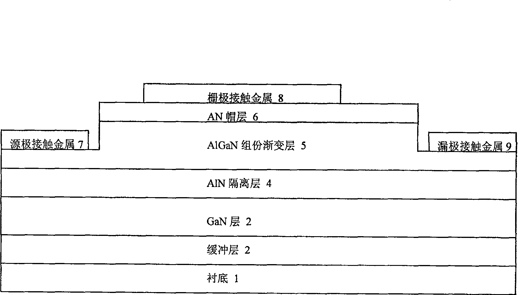
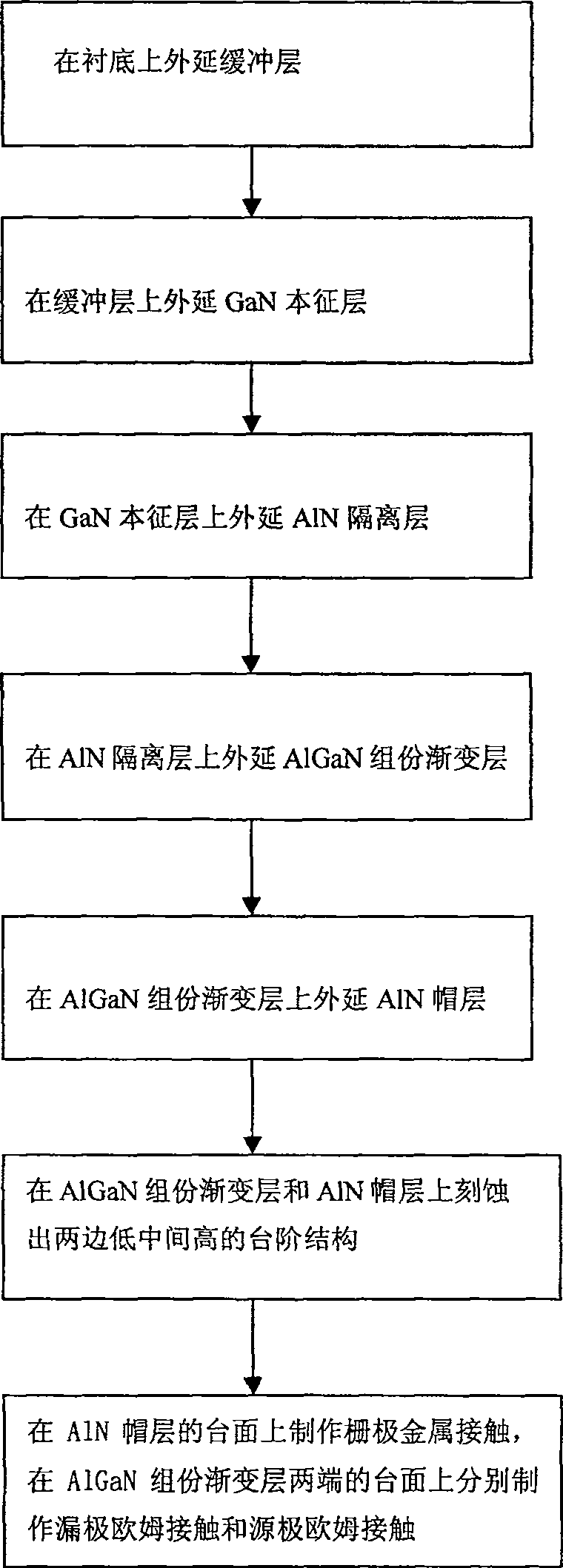
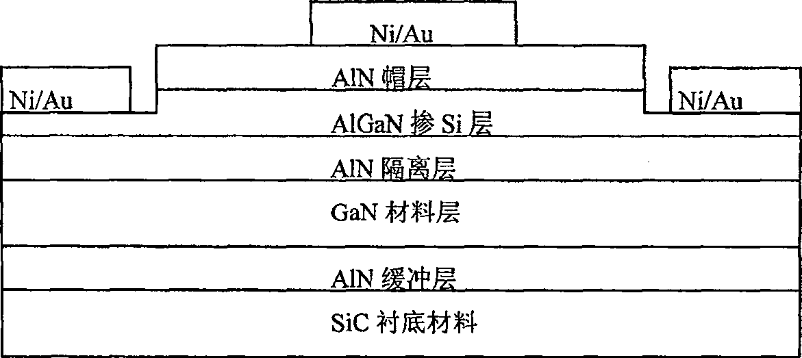
[0038] The process of manufacturing a high-power GaN MISFET device of a silicon carbide substrate by using the method of the invention.

[0039] In the first step, a layer of AlN material with a thickness of 50 nanometers is deposited on the SiC substrate material by using the MOCVD method at a temperature of 1050 degrees and a pressure of 20 Torr, as a buffer layer for subsequent growth of GaN materials.

[0040] In the second step, a GaN intrinsic layer with a thickness of 2 microns is deposited on the buffer layer by using MOCVD technology at a temperature of 1000 degrees and a pressure of 20 Torr.

[0041] The third step is to deposit an AlN material layer with a thickness of 1 nanometer on the GaN intrinsic layer by using MOCVD technology at a temperature of 1000 degrees and a pressure of 20 Torr.

[0042] The fourth step is to use MOCVD technology on the AlN material layer to deposit an AlGaN composition graded material layer with a thickness of 10 nanometers and an Al c...

Embodiment 2

[0047] A high-power GaN MISFET device process of manufacturing a sapphire substrate by using the method of the invention.

[0048] The first step is to use MOCVD technology on the sapphire substrate material to deposit a layer of GaN material with a thickness of 100 nanometers at a temperature of 550 degrees and a pressure of 40 Torr as a buffer layer for subsequent growth of GaN materials.

[0049] In the second step, a GaN intrinsic layer with a thickness of 3 microns is deposited on the buffer layer using MOCVD technology at a temperature of 900 degrees and a pressure of 40 Torr.

[0050] In the third step, an AlN isolation layer with a thickness of 2 nanometers is deposited on the GaN intrinsic layer by using MOCVD technology at a temperature of 1000 degrees and a pressure of 20 Torr.

[0051] The fourth step is to use MOCVD technology on the AlN isolation layer to deposit an AlGaN graded layer with a thickness of 15 nanometers and an Al composition that gradually changes ...


PUM


Abstract

The invention discloses a GaN device and a preparation method based on a composition gradient GaN MISFET. The device includes bottom layer (1), buffer layer (2), intrinsic GaN material layer (3), AlN isolation layer (4) and source (7), drain (8), gate (9) electrode contacts, wherein AlN isolation An AlGaN composition graded layer (5) and an AlN cap layer (6) are sequentially arranged on the layer. The manufacturing process of the device is to sequentially epitaxially GaN or AlN buffer layer, deposit GaN intrinsic layer, deposit AlN spacer layer on sapphire or silicon carbide substrate; deposit AlGaN composition graded layer, deposit AlN cap layer, and Parts of both sides of the top AlN cap layer and both sides of the AlGaN gradient layer are respectively etched away to form a stepped structure with a height in the middle and low sides on both sides, and the ohmic contacts and gates of the source and drain are respectively made on different mesas of the steps. Pole metal contact. The invention has the advantages of small leakage current and high gate voltage, and can be used for making high-power microwave devices.

Description

technical field [0001] The invention belongs to the technical field of microelectronics, and relates to a semiconductor device structure and a manufacturing method, in particular to a GaN device based on a composition gradient GaN MISFET and a preparation method, which can be used in the manufacture of high-power GaN devices. Background technique [0002] In recent years, the third-generation wide-bandgap semiconductor materials represented by SiC and GaN have large bandgap width, high critical field strength, high thermal conductivity, high carrier saturation rate, and high concentration of two-dimensional electron gas at the heterojunction interface. Its excellent characteristics have attracted widespread attention from people. In theory, high electron mobility transistor HEMT, heterojunction bipolar transistor HBT, light-emitting diode LED, laser diode LD and other devices made of these materials will have excellent performance that cannot be compared with existing device...

Claims


Application Information

Patent Timeline
Patent Type & Authority Patents(China)
IPC IPC(8): H01L29/778H01L29/45H01L29/201H01L21/335H01L21/28
Inventor 郝跃陈军峰张进城
Owner XIDIAN UNIV
Why Eureka
Try Eureka