Target components and processing methods

A processing method and target material technology, applied in metal material coating process, vacuum evaporation plating, coating, etc., can solve problems such as abnormal discharge of sandblasting line, affecting the production process of semiconductor chips, and the sputtering process cannot be carried out normally.

Active Publication Date: 2019-10-18
KONFOONG MATERIALS INTERNATIONAL CO LTD
View PDF5 Cites 0 Cited by
  • Summary
  • Abstract
  • Description
  • Claims
  • Application Information

AI Technical Summary

Problems solved by technology

However, in the prior art, due to the limitations of the sandblasting process, the sandblasting line (that is, the boundary line of the sandblasting area) often appears irregular. During the sputtering of the target, the irregular sandblasting The line will cause abnormal discharge and other phenomena, and even cause the sputtering process to fail to proceed normally, seriously affecting the production process of semiconductor chips

Method used


Image

  • Target components and processing methods
  • Target components and processing methods
  • Target components and processing methods

Examples


no. 1 example

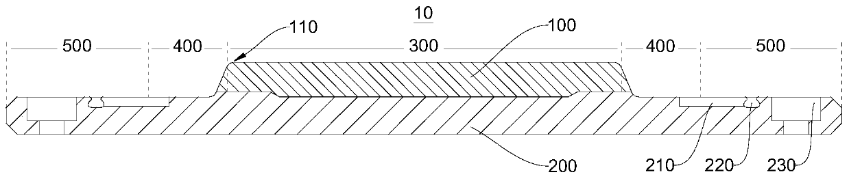
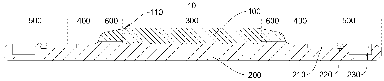
[0040] figure 1 It shows a schematic structural view of the first target assembly 10 provided by the embodiment of the present invention under a first viewing angle, figure 2A schematic structural view of the first target assembly 10 provided by the embodiment of the present invention under the second viewing angle is shown. The target assembly 10 is used for sputtering coating in the semiconductor chip manufacturing process. combined reference figure 1 as well as figure 2 , the target assembly 10 includes a target 100 and a back plate 200 for carrying the target 100 . The target assembly 10 is usually made of metal, alloy, ceramics and other materials. For example, the target 100 is made of titanium, and the back plate 200 is made of aluminum. Of course, this is only a relatively common combination of materials. The target 100 and The backplane 200 can also use other combinations of materials.

[0041] Wherein, the surface of the target 100 includes a front, a back and...

no. 2 example

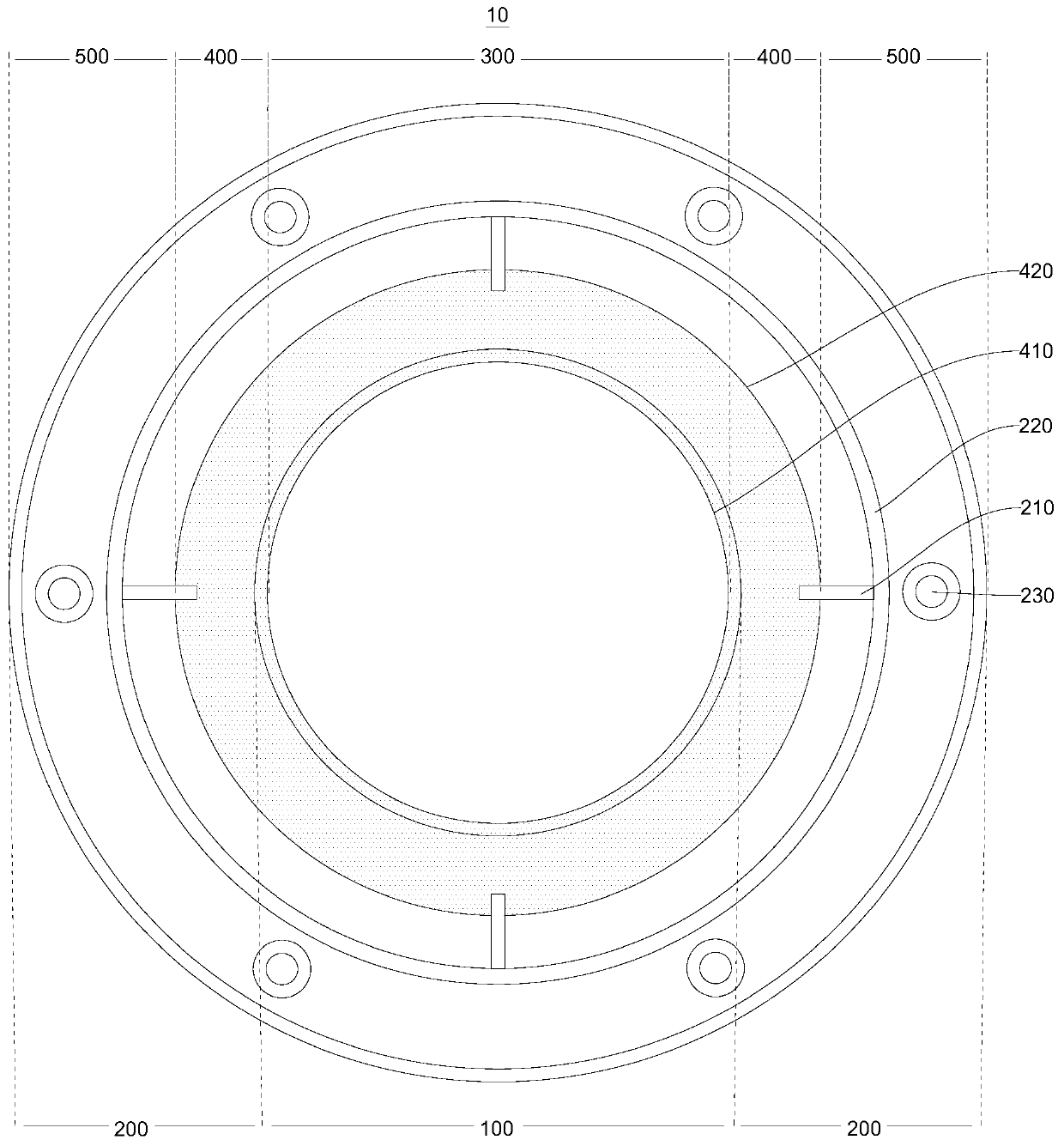
[0054] The embodiment of the present invention also provides a target assembly processing method for processing the target assembly 10 provided in the embodiment of the present invention, the method includes: fixing the target assembly 10; Turning is carried out until each point on the first sandblasting line 410 has the same distance to the center point of the sputtering surface 300; the second sandblasting line 420 of the sandblasting area 400 is turned until the distance between the points on the second sandblasting line 420 The distances from each point to the center point of the sputtering surface 300 are the same.

[0055] Further, before the step of turning the first sandblasting line 410 of the sandblasting area 400 until the distances from each point on the first sandblasting line 410 to the center point of the sputtering surface 300 are the same, the method further includes: The R angle 110 is turned at the boundary position between the sputtering surface 300 and the...


PUM


Abstract

The invention relates to the technical field of machining, and provides a target component and a processing method. The target component comprises a target and a backing plate used for bearing the target, wherein the surface of the target comprises a front side, a back side and sides, and the front side of the target is the sputtering surface of the target; and the back side of the target is opposite to the front side of the target, and the sides of the target are adjacent to the front side and the back side of the target separately. Meanwhile, the back side of the target is connected to the front side of the backing plate, and the sides of the target are adjacent to the front side of the backing plate; and the junction positions between the sides of the target and the front side of the backing plate are provided with sand blasting areas formed through sand blasting treatment and surrounding the sputtering surface, and the distances between the points of the same sand blasting line ofthe sand blasting areas and the center point of the sputtering surface are the same, wherein the sand blasting lines are the boundary lines of the sand blasting areas. The sand blasting areas of the target component have tidy sand blasting lines, so that abnormal sputtering is not generated in the sputtering process of the target, and semiconductor chips can be produced smoothly.

Description

technical field [0001] The invention relates to the field of mechanical processing, in particular to a target component and a processing method. Background technique [0002] The peripheral area of ​​the sputtering surface of the sputtering target is usually sandblasted to form a rough sandblasted area to absorb impurities generated during the sputtering process of the target and improve the sputtering performance of the target. However, in the prior art, due to the limitations of the sandblasting process, the sandblasting line (that is, the boundary line of the sandblasting area) often appears irregular. During the sputtering of the target, the irregular sandblasting Lines will cause abnormal discharge and other phenomena, and even cause the sputtering process to fail to proceed normally, seriously affecting the production process of semiconductor chips. Contents of the invention [0003] In view of this, embodiments of the present invention provide a target component an...

Claims


Application Information

Patent Timeline
Patent Type & Authority Patents(China)
IPC IPC(8): C23C14/34B23B1/00
Inventor 姚力军潘杰王学泽张良进
Owner KONFOONG MATERIALS INTERNATIONAL CO LTD
Why Eureka
Try Eureka