A method for preparing ito nanowires and gas sensors thereof by sputtering with high radio frequency power
A technology of radio frequency power and nanowires, which is applied in the field of gas sensor to achieve the effects of stable performance, simple preparation process and low preparation cost
- Summary
- Abstract
- Description
- Claims
- Application Information
AI Technical Summary
Problems solved by technology
Method used
Image
Examples
Embodiment 1
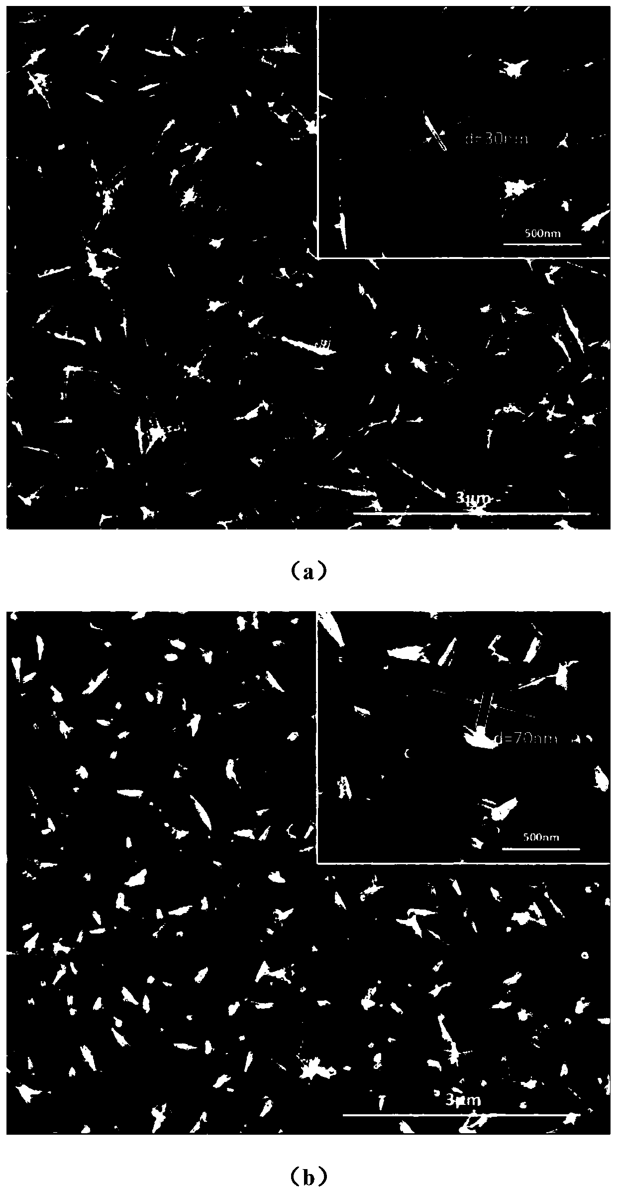
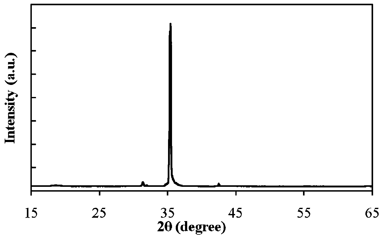
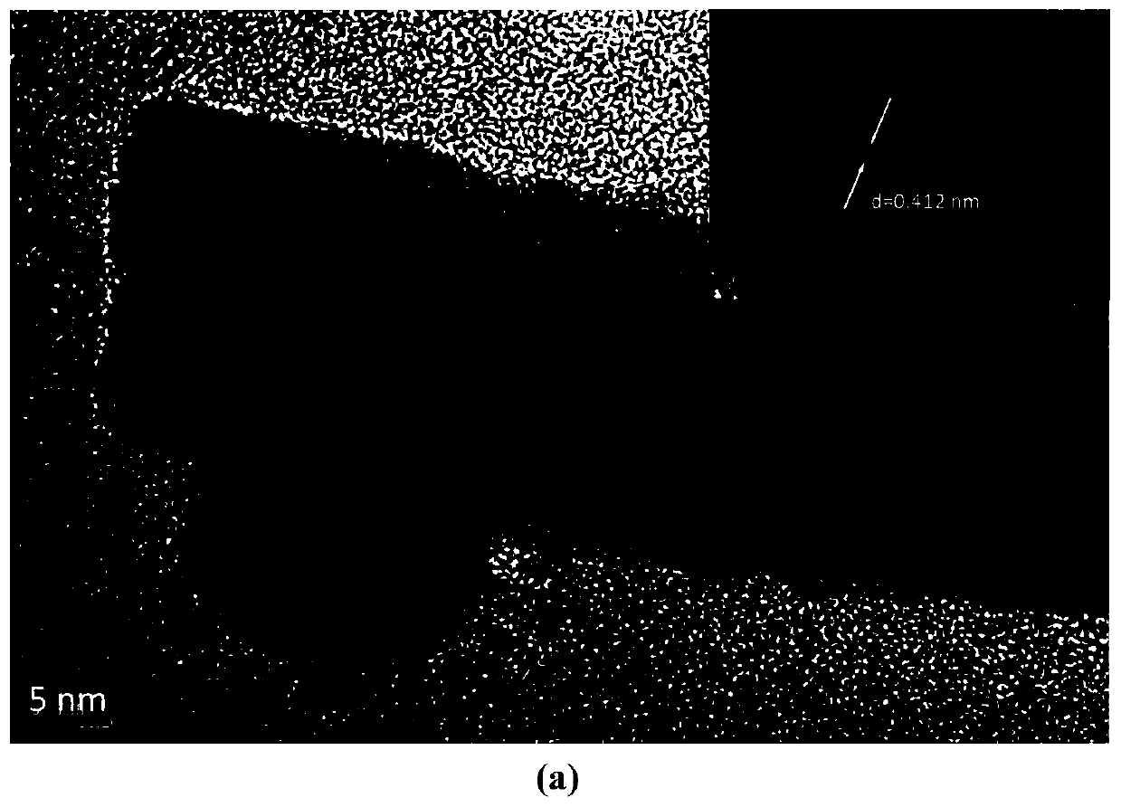
[0030] The key of the invention lies in the preparation of ITO nanowires by high radio frequency power magnetron sputtering. In order to prepare ITO nanowire gas sensors with good performance, it is necessary to continuously adjust the process parameters of magnetron sputtering, so that the growth of nanowires can be carried out without a catalyst.
[0031] The invention provides a method for preparing ITO nanowires and gas sensors thereof by using high radio frequency power, the specific steps comprising:
[0032] (1) The silicon substrate is placed in a mixed solution of concentrated sulfuric acid and hydrogen peroxide (H 2 SO 4 :H 2 o 2 =3:1) for 0.5 hours, then rinsed with deionized water, and finally dried with nitrogen;
[0033] (2) Place the processed silicon substrate on the tray of the sputtering chamber, heat it to 500°C, keep it warm for 30 minutes, and pass a mixed gas of argon and oxygen (Ar 2 :O 2 =25sccm:0.2sccm), the sputtering chamber pressure was set to...
Embodiment 2
[0036] Embodiment 2: Gas sensor preparation method
[0037] A remarkable feature of the present invention is that it can realize the preparation of ITO nanowires on ceramic tubes in one step, and the specific implementation steps are as follows:
[0038] (1) Place the ceramic tube in the alcohol solution for 0.5 hours and then dry it with nitrogen;
[0039] (2) Place the ceramic tube on the sputtering chamber tray, adjust the magnetron sputtering process parameters: the radio frequency power is 250W, the mixed gas ratio of argon and oxygen is Ar2:O2=25sccm:0.2sccm, and the sputtering chamber pressure is set is 1Pa, and the temperature is 500°C;
[0040] (3) After the chamber temperature reaches 500°C, the holding time is 30 minutes;
[0041] (4) The sputtering time is 0.5 hours, then naturally cooled to room temperature;
[0042] (5) Take out the ceramic tube, and rapidly anneal at 470°C for 5 minutes in an air atmosphere;
[0043] (6) The lead wires are connected to the c...
PUM
| Property | Measurement | Unit |
|---|---|---|
| size | aaaaa | aaaaa |
| length | aaaaa | aaaaa |
| lattice spacing | aaaaa | aaaaa |
Abstract
Description
Claims
Application Information
 - R&D
- Intellectual Property
- Life Sciences
- Materials
- Tech Scout
- Unparalleled Data Quality
- Higher Quality Content
- 60% Fewer Hallucinations
Browse by: Latest US Patents, China's latest patents, Technical Efficacy Thesaurus, Application Domain, Technology Topic, Popular Technical Reports.
© 2025 PatSnap. All rights reserved.Legal|Privacy policy|Modern Slavery Act Transparency Statement|Sitemap|About US| Contact US: help@patsnap.com


