OLED display device and preparation method thereof

A display device, a technology directly above, applied in the manufacture of semiconductor/solid-state devices, electrical components, electrical solid-state devices, etc., can solve the problems that the film layer is prone to breakage, does not meet the requirements, and the water-oxygen permeability is high, so as to reduce the permeability , improve the service life and avoid the effect of package failure

Inactive Publication Date: 2018-09-21
TCL CHINA STAR OPTOELECTRONICS TECH CO LTD
View PDF4 Cites 5 Cited by
  • Summary
  • Abstract
  • Description
  • Claims
  • Application Information

AI Technical Summary

Problems solved by technology

[0003] However, the structure of the current OLED display device adopts such as figure 1 The shown thin film encapsulation method is carried out, 1', 2', 3', 4', 5', 6', 7', 8' respectively represent the glass substrate, TFT (Thin Film Transistor, thin film transistor) layer, pixel layer , the first barrier layer, the first buffer layer, the second barrier layer, the second buffer layer, and the third barrier layer, but due to the thin film packaging barrier layer and buffer layer and other film layers are thin, and there is stress between the film layers, so , the ability of the barrier layer and the buffer layer to block water and oxygen has not achieved the desired effect, the water-oxygen permeability is high, and the film layer of the barrier layer and the buffer layer is more prone to breakage, resulting in package failure

Method used


Image

  • OLED display device and preparation method thereof
  • OLED display device and preparation method thereof
  • OLED display device and preparation method thereof

Examples


Embodiment Construction

[0036] The invention provides a method for preparing an OLED display device, comprising the following steps:

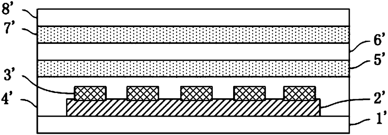
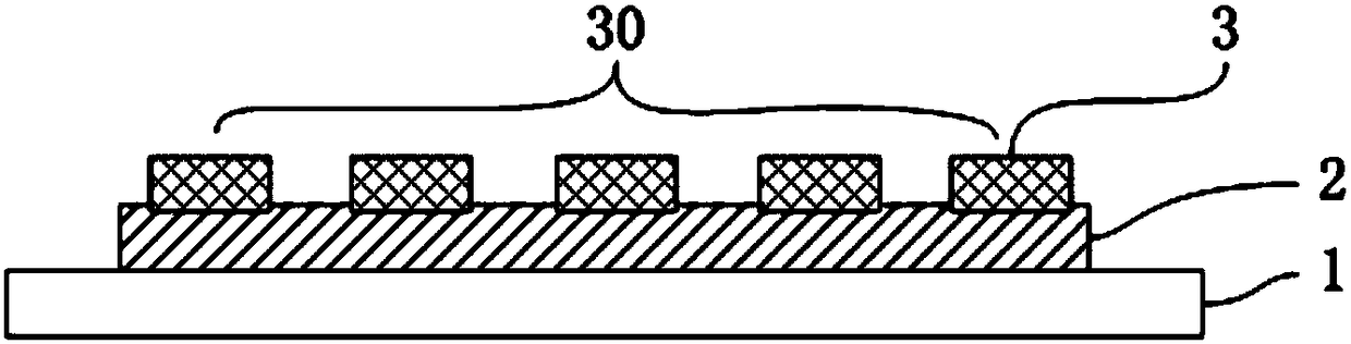
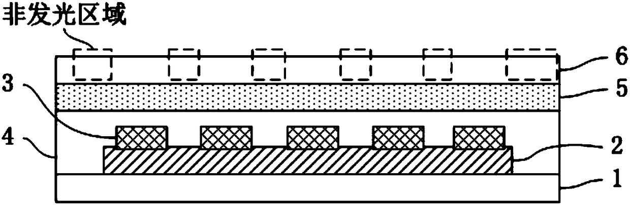
[0037] Such as figure 2 As shown, a TFT (Thin Film Transistor, thin film transistor) layer 2 is prepared on a glass substrate 1; the TFT layer 2 includes a plurality of TFTs to form a driving circuit, which can drive the OLED device to emit light;

[0038] Prepare an OLED (Organic Light-Emitting Diode, organic light-emitting diode) device layer 30 on the TFT layer 2, prepare a barrier layer and a buffer layer on the glass substrate 1, and the barrier layer covers the OLED device layer 30; generally speaking, the barrier layer is used For shielding water vapor and oxygen; here, the barrier layer and the buffer layer constitute the thin film encapsulation layer;

[0039] A plurality of grooves 61 are prepared on the barrier layer, and a water-absorbing material layer 7 is prepared in the plurality of grooves 61; here, the water-absorbing material layer 7 can be used t...


PUM


Abstract

The invention provides an OLED display device and a preparation method thereof. The method comprises a step of preparing a TFT layer on a glass substrate, a step of preparing an OLED device layer on the TFT layer, a step of preparing a barrier layer and a buffer layer on the glass substrate, wherein the barrier layer covers the OLED device layer, a step of preparing a plurality of grooves on the barrier layer and preparing water absorbing material layers in the grooves. According to the OLED display device and the preparation method, the permeability of water and oxygen is reduced, the risk ofthe breakage of the barrier layer and the buffer layer is reduced, and the service life of the OLED display device is improved.

Description

technical field [0001] The invention relates to the field of display technology, in particular to an OLED display device and a preparation method thereof. Background technique [0002] In the current field of lighting and display, due to the characteristics of OLED (Organic Light-Emitting Diode, Organic Light-Emitting Diode), such as low start-up voltage, light and thin, and self-illumination, more and more researches are widely used to develop lighting products. As well as in the panel industry to meet the needs of low energy consumption, thinness and surface light source. At present, OLED flexible display panels are flexible, thin, and self-illuminating, leading to the birth of more and more OLED flexible display products. [0003] However, the structure of the current OLED display device adopts such as figure 1 The shown thin film encapsulation method is carried out, 1', 2', 3', 4', 5', 6', 7', 8' respectively represent the glass substrate, TFT (Thin Film Transistor, th...

Claims


Application Information

Patent Timeline
Patent Type & Authority Applications(China)
IPC IPC(8): H01L51/56H01L27/32H01L51/52
CPCH10K59/12H10K50/846H10K71/00H10K50/844
Inventor 黄辉
Owner TCL CHINA STAR OPTOELECTRONICS TECH CO LTD
Why Eureka
Try Eureka