Power device with surface charge region structure

A surface charge and power device technology, applied in electrical components, semiconductor devices, circuits, etc., can solve the problems of high cost and complex process, achieve good process tolerance, simple and feasible process, and improve the effect of lateral withstand voltage

Active Publication Date: 2018-09-18
GUILIN UNIV OF ELECTRONIC TECH
View PDF10 Cites 0 Cited by
  • Summary
  • Abstract
  • Description
  • Claims
  • Application Information

AI Technical Summary

Problems solved by technology

The traditional means of improving the withstand voltage are often complicated in process and high in cost and price. The surface charge region structure is adopted, the process is simple and feasible, the process tolerance is good, and it is compatible with the conventional CMOS process

Method used


Image

  • Power device with surface charge region structure
  • Power device with surface charge region structure

Examples


Embodiment 1

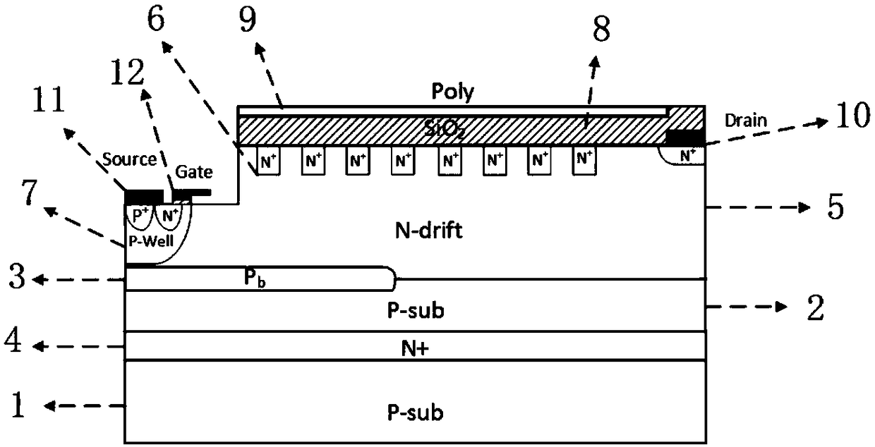
[0032] like figure 1 The shown power device with a surface charge region structure includes a drift region 5, a substrate II2, a floating equipotential layer 4, and a substrate I1 arranged sequentially from top to bottom; an N+ drain region is arranged on the drift region 5 , drain electrode 10, gate electrode 12, source electrode 11, N+ contact region, P well 7 and P+ source region; the top of the drift region 5 is provided with N + charge region 6, the N + A surface substrate 9 is arranged above the charge region 6; the N + The charge regions 6 are uniformly distributed along the lateral direction. The positions of the gate electrode 12 and the source electrode 11 are lower than the surface substrate 9 .

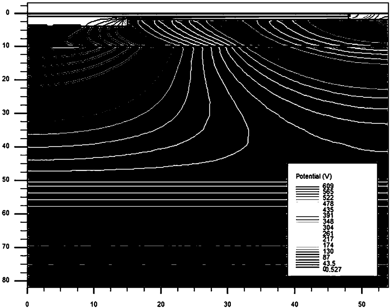
[0033] Since a series of equidistant N + charge region 6, so the surface charge region is in the adjacent N + The interface charge is generated in the charge interval, which enhances the surface lateral electric field and improves the surface lateral withstand voltage...


PUM


Abstract

The invention provides a power device with a surface charge region structure, and the power device comprises a P substrate I (1), a floating equipotential layer (4), a P substrate II (2) and a drift region (5), wherein the P substrate I (1), the floating equipotential layer (4), the P substrate II (2) and the drift region (5) are arranged in order from the bottom to the top. The drift region (5) is provided with an N+ drain region, a drain electrode (10), a gate electrode (12), a source electrode (11), an N+ contact region, a P well (7), and a P+ source region. A series of laterally and equidistantly distributed N+ charge regions (6) are disposed at the top of the drift region (5) and within the drift region to form the surface charge region. Because the surface of the drift region is provided with a surface charge region structure of a series of equidistantly distributed N+ charge regions, the surface charge region generates interface charges, and the electric field in the charge region is improved, and the lateral withstand voltage of the device is improved. The interface charge improves the longitudinal electric field and longitudinal withstand voltage of a buried layer at the same time, reduces the electric field nearby the drain electrode and prevents the surface of the device from being broken down too early. Because the power device employs the surface charge region structure of equidistantly distributed N+ charge regions, the power device is simple and feasible in technology, is better in technological tolerance, and is compatible with the conventional CMOS technology.

Description

technical field [0001] The invention relates to the technical field of semiconductor power devices, in particular to a power device with a surface charge region structure. Background technique [0002] Power semiconductor device is a semiconductor device for power processing, and it is the main object of power electronics research. Power electronics was born under the impetus of the development of power semiconductor devices, and has gradually matured after decades of development. Power semiconductor devices have a wide range of applications such as weaponry, power electronics, aerospace, flat panel display drivers and other high-tech industries. However, lateral power devices have lateral channels, and the drain, source, and gate are all on the chip surface, which is easy to integrate with low-voltage signals through internal connections, and is widely used in power integrated circuits. Therefore, domestic and foreign experts and scholars have invested great attention and...

Claims


Application Information

Patent Timeline
Patent Type & Authority Applications(China)
IPC IPC(8): H01L29/786H01L29/06
CPCH01L29/0623H01L29/78606
Inventor 李琦张昭阳李海鸥陈永和张法碧傅涛鲍婷婷
Owner GUILIN UNIV OF ELECTRONIC TECH
Why Eureka
Try Eureka