Display substrate and manufacturing method and display device thereof

A display substrate and a display device technology are applied in the fields of display devices, display substrates and manufacturing methods thereof, which can solve problems such as low yield rate, and achieve the effects of high yield rate, avoiding GDS phenomenon and good ductility.

Pending Publication Date: 2018-09-07
BOE TECH GRP CO LTD +1
View PDF5 Cites 11 Cited by
  • Summary
  • Abstract
  • Description
  • Claims
  • Application Information

AI Technical Summary

Problems solved by technology

[0004] Embodiments of the present invention provide a display substrate, a manufacturing method thereof, and a display device, which can solve the problems of GDS phenomenon on the display substrate and low yield rate in the related art. The technical solution is as follows:

Method used


Image

  • Display substrate and manufacturing method and display device thereof
  • Display substrate and manufacturing method and display device thereof
  • Display substrate and manufacturing method and display device thereof

Examples


Embodiment Construction

[0039] In order to make the object, technical solution and advantages of the present invention clearer, the implementation manner of the present invention will be further described in detail below in conjunction with the accompanying drawings.

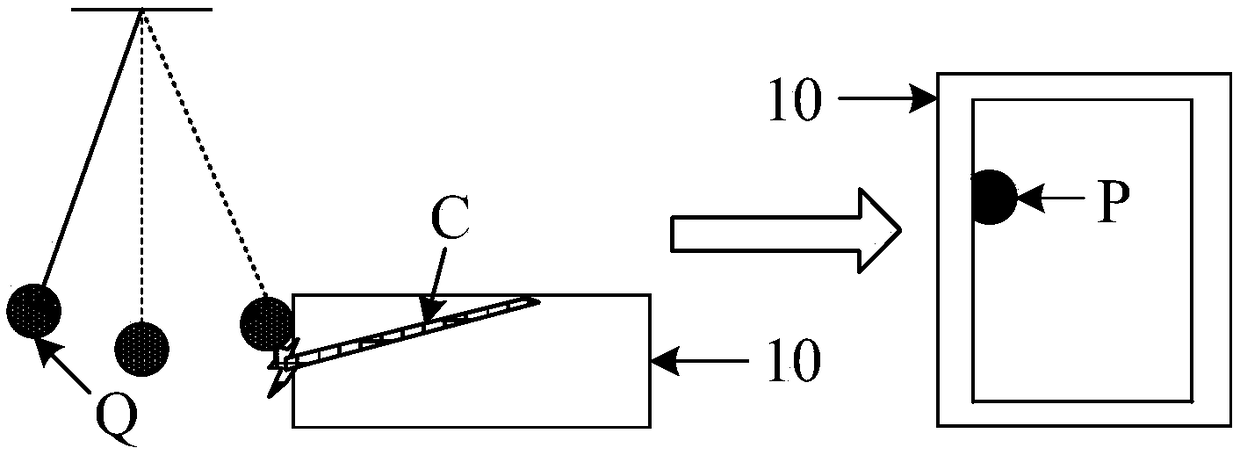
[0040] In order to ensure the yield rate of the display substrate when it leaves the factory, testers will conduct a series of performance tests on the display substrate after the display substrate is manufactured. figure 1 A schematic diagram is shown when a tester performs an impact test on a flexible display substrate. refer to figure 1 , when the tester hits the edge of the display substrate 10 with a ball Q, a crack C appears on the edge of the display substrate 10, and the crack C gradually extends to the packaging area of ​​the display substrate 10, which may cause the packaging failure of the display substrate. At this time, water vapor or oxygen may intrude into the effective display area inside the display substrate 10 throu...


PUM


Abstract

The invention discloses a display substrate and a manufacturing method and a display device thereof, and belongs to the technical field of display. The provided display substrate comprises a substratum substrate and an obstructing structure arranged on the substratum substrate. It is due to the fact that the provided obstructing structure is made from metal materials with higher hardness, better ductility and stronger impact resistance, the obstructing structure is located at a non-display area of the substratum substrate, and a gap is reserved between the obstructing structure and a packagingarea, the obstructing structure can effectively avoid the problems that a split of the edge of the display substrate extends to the packaging area so as to cause packaging failure, and moisture or oxygen entering an effective display area causes the GDS phenomenon appearing on the display substrate. The yield of the display substrate is higher, and the quality is better.

Description

technical field [0001] The invention relates to the field of display technology, in particular to a display substrate, a manufacturing method thereof, and a display device. Background technique [0002] A display substrate is a product that can emit light autonomously or passively in the field of display technology. [0003] The impact resistance of the display substrate in the related art is relatively poor. When the edge of the display substrate is deformed by external impact, the edge of the display substrate is prone to cracks. If the crack extends to the packaging area of ​​the display substrate, it may cause the display substrate packaging fail. At this time, water vapor or oxygen in the air may invade the interior of the display substrate through the crack, causing growing black spots (Growing Black Spots, GDS) to appear on the display substrate, which seriously affects the yield and quality of the display substrate. quality. Contents of the invention [0004] Em...

Claims


Application Information

Patent Timeline
IPC IPC(8): G02F1/1333G09F9/00H01L27/32
CPCG02F1/1333G09F9/00H10K59/12H10K71/00H10K59/873H10K59/88H10K50/844H10K50/115H10K59/131H10K59/1201
Inventor 吕浩铭
Owner BOE TECH GRP CO LTD
Why Eureka
Try Eureka