Wafer processing method

A processing method and wafer technology, which is applied in the manufacture of electrical components, semiconductor/solid-state devices, circuits, etc., can solve problems such as wafer defects, prevent fragments, avoid spherical defects, and improve product yield.

Inactive Publication Date: 2018-09-04
SHANGHAI HUALI MICROELECTRONICS CORP
View PDF9 Cites 3 Cited by
  • Summary
  • Abstract
  • Description
  • Claims
  • Application Information

AI Technical Summary

Problems solved by technology

[0005] The object of the present invention is to provide a wafer processing method to solve the problem of wafer defects in the process

Method used


Image

  • Wafer processing method

Examples


Embodiment Construction

[0018] In order to make the objects, features and advantages of the present invention more comprehensible, please refer to the accompanying drawings. It should be noted that the structures, proportions, sizes, etc. shown in the drawings attached to this specification are only used to match the content disclosed in the specification, for those who are familiar with this technology to understand and read, and are not used to limit the implementation of the present invention. Limiting conditions, so there is no technical substantive meaning, any modification of structure, change of proportional relationship or adjustment of size, without affecting the effect and purpose of the present invention, should still fall within the scope of the present invention. The disclosed technical content must be within the scope covered.
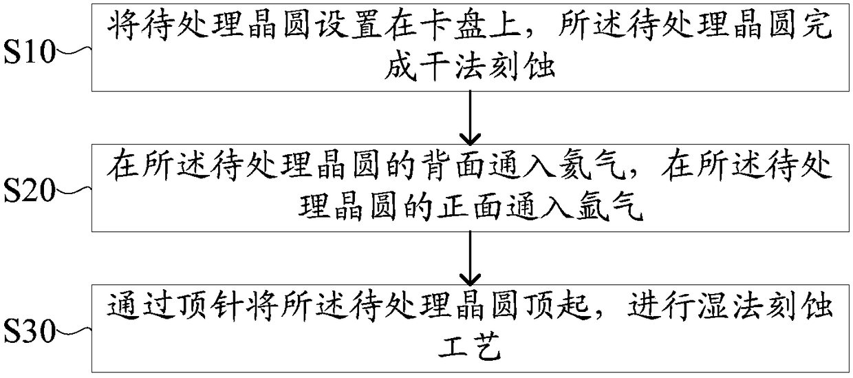
[0019] The core idea of ​​this application is to solve the wafer processing between dry etching and wet etching, effectively solve the static electricity residu...


PUM


Abstract

The invention provides a wafer processing method. The wafer processing method comprises the steps of enabling a to-be-processed wafer to be placed on a chuck, and completing dry etching on the to-be-processed wafer; pumping helium to the back surface of the to-be-processed wafer, and pumping argon to the front surface of the to-be-processed wafer; enabling the to-be-processed wafer to be ejected by an ejector pin; and performing a wet etching process. According to the wafer processing method, after dry etching is completed on the to-be-processed wafer, helium is pumped to the back surface of the to-be-processed wafer; when the wafer is cooled, a carrier for transferring electrostatic charges removes electrostatic charges from the to-be-processed wafer; then the front surface of the to-be-processed wafer is pumped with argon to take away the electrostatic charges from the surface of the wafer; and next, the to-be-processed wafer is ejected by the ejector pin, so that dynamic alignment offset can be relieved, risk of wafer fragmenting caused by overhigh dynamic alignment offset can be prevented, and spherical defects formed in the wet etching can be avoided effectively, thereby improving product yield.

Description

technical field [0001] The invention relates to the technical field of semiconductor manufacturing, in particular to a wafer processing method. Background technique [0002] Semiconductor manufacturing technology requires a variety of different physical and chemical processes on the wafer to form the device structure. The wafer is passed on the chuck, and the etching process is one of the most important processes. The etching process also includes dry etching and wet etching. The mainstream dry etching usually uses etching process conditions such as high power and high plasma density to form a high etching rate, thereby obtaining high wafer output. , After the dry etching process is completed, the etching chamber and the surface of the wafer usually have more charges. In addition, if the etching is a film layer with insulating properties, it will cause difficulty or insufficient release of residual charges. [0003] When wet etching is performed after dry etching, the char...

Claims


Application Information

Patent Timeline
Patent Type & Authority Applications(China)
IPC IPC(8): H01L21/3105H01L21/687
CPCH01L21/3105H01L21/68714
Inventor 刘庆王福喜昂开渠任昱吕煜坤朱骏
Owner SHANGHAI HUALI MICROELECTRONICS CORP
Why Eureka
Try Eureka