
A preparation method for realizing cu-doping of topological insulator bismuth selenide nanomaterials

A technology of topological insulators and nanomaterials, applied in nanotechnology, nanotechnology, binary selenium/tellurium compounds, etc., can solve the problems of inconvenience of topological superconductors, poor crystallinity of products, complicated processes, etc., and achieve low cost, high crystallinity, simple steps

Inactive Publication Date: 2020-06-19
TIANJIN UNIVERSITY OF TECHNOLOGY
View PDF7 Cites 0 Cited by
  • Summary
  • Abstract
  • Description
  • Claims
  • Application Information

AI Technical Summary

Problems solved by technology

In the preparation methods of bismuth selenide to achieve Cu doping, there are electrochemical methods, hot wall epitaxy, and molecular beam epitaxy, but most of them have the problems of complex process, poor product crystallinity, and low purity. It is inconvenient, it is of great significance to perfect and optimize the preparation method of Cu-doped bismuth selenide nanomaterials

Method used


Image

  • A preparation method for realizing cu-doping of topological insulator bismuth selenide nanomaterials
  • A preparation method for realizing cu-doping of topological insulator bismuth selenide nanomaterials
  • A preparation method for realizing cu-doping of topological insulator bismuth selenide nanomaterials

Examples


Embodiment 1

[0020] Prepare Cu-doped bismuth selenide nanomaterial according to the method provided by the invention, the steps are as follows:

[0021] (1) Clean SiO 2 / Si substrate, and use magnetron sputtering on SiO 2 Coating a layer of Cu film on the / Si substrate, and then coating a layer of Au film on the Cu film, the thickness of the Cu film and the Au film are both 10nm, as the Au / Cu catalyst;

[0022] (2) Place the cleaned quartz tube (with an inner diameter of 50 mm and a length of 1.5 m) horizontally in the tube furnace, and place bismuth selenide with a mass of 0.02 to 0.03 g and a weight ratio concentration of 99.999% at the heating center Powder (AlfaAsear), the SiO obtained in step (1) is placed at 8-14 cm away from the bismuth selenide powder in the downstream direction of the carrier gas 2 / Si substrate, sealed to the quartz tube, the sealing method is flange sealing, and vacuumized by a mechanical pump, the pressure is ≤130Pa;

[0023] (3) Heat the tube furnace in ste...

Embodiment 2

[0030] Prepare Cu-doped bismuth selenide nanomaterial according to the method provided by the invention, the steps are as follows:

[0031] (1) Clean SiO 2 / Si substrate, and use magnetron sputtering on SiO 2 Coating a layer of Cu film on the / Si substrate, and then coating a layer of Au film on the Cu film, the thickness of the Cu film and the Au film are both 10nm, as the Au / Cu catalyst;

[0032] (2) Place the cleaned quartz tube (with an inner diameter of 50 mm and a length of 1.5 m) horizontally in the tube furnace, and place bismuth selenide with a mass of 0.02 to 0.03 g and a weight ratio concentration of 99.999% at the heating center Powder (AlfaAsear), the SiO obtained in step (1) is placed at 8-14 cm away from the bismuth selenide powder in the downstream direction of the carrier gas 2 / Si substrate, sealed to the quartz tube, the sealing method is flange sealing, and vacuumized by a mechanical pump, the pressure is ≤130Pa;

[0033] (3) Heat the tube furnace in ste...

Embodiment 3

[0037] The difference between this embodiment and embodiment 1 is that the heating temperature in step (3) is set to 600° C., and the others are the same as embodiment 1.


PUM

PropertyMeasurementUnit
Lengthaaaaaaaaaa

Abstract

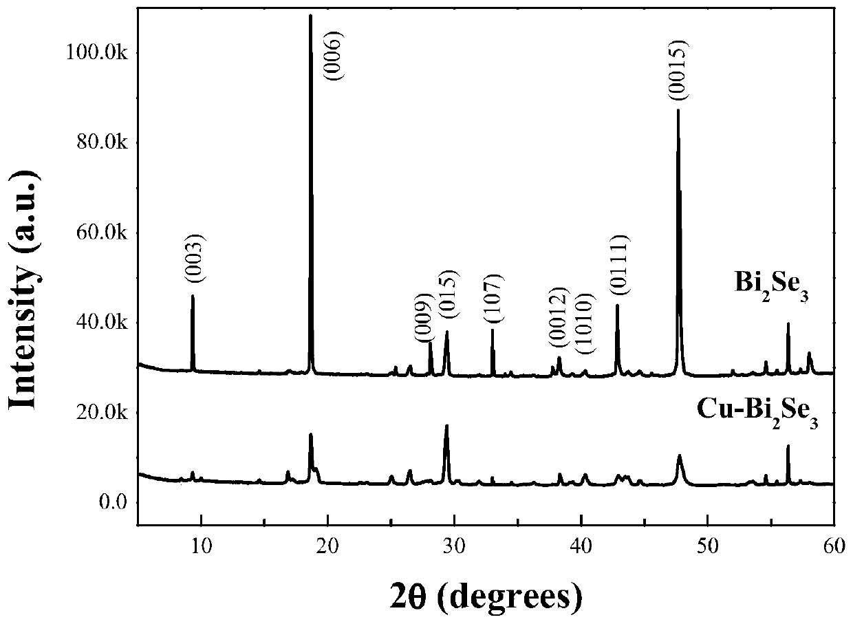
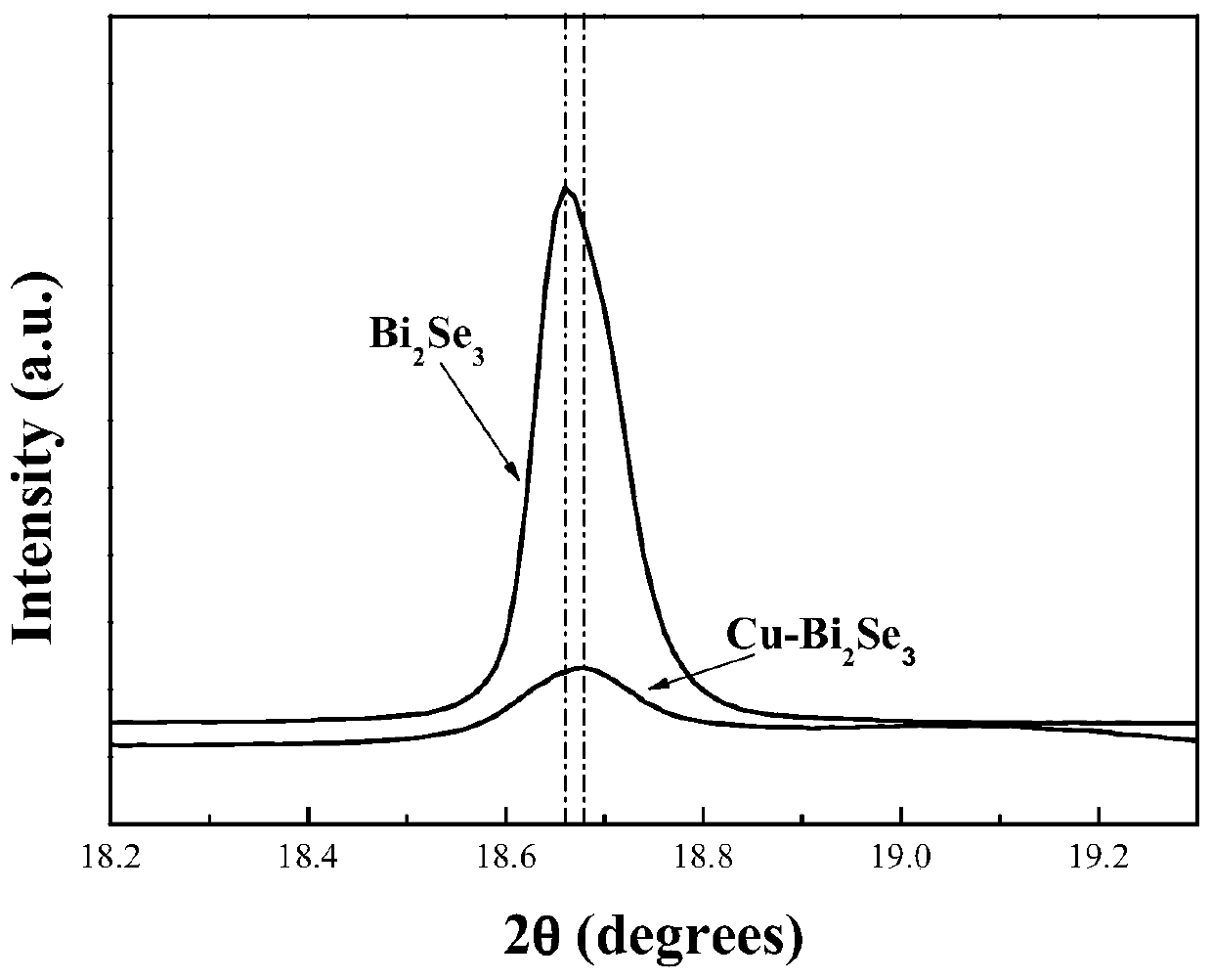
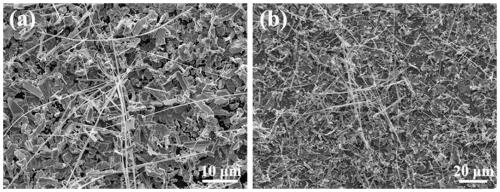
The invention discloses a preparation method for Cu doping of bismuth selenide nano-materials of a topology insulator, and the nano-materials are a nano-wire and a nano-strip. The method comprises thesteps: employing a vapour deposition method, taking bismuth selenide as a raw material, carrying out the high-temperature evaporation in a tube furnace, carrying out the transmission through inertialcarrying gas, and preparing the Cu-doped bismuth selenide nano-materials under the condition of taking an Au / Cu film as a catalyst. The prepared materials are good in crystallinity, and the lengths of the nano-wire and the nano-strip are at the level of hundreds of micrometers. The X-ray diffraction analysis (XRD), X-ray energy dispersion spectrum (EDS) and X-ray excited Auger electron spectrum (XAES) are employed for indicating the introduction of Cu and the valence state of doped Cu.

Description

technical field [0001] The invention relates to a preparation method for Cu-doped bismuth selenide nanometer material, which belongs to the field of semiconductor materials and microelectronic devices. Background technique [0002] Bismuth selenide is a narrow-bandgap semiconducting semiconductor material, which has attracted extensive attention due to its good pyroelectric properties and infrared detection effect. In recent years, theoretical calculations and experimental work have proved that bismuth selenide is a strong three-dimensional topological insulator, that is, there is an insulating state with a gap in the body, and a conductive metal state on the surface, and electrons are transported on the surface in a spin-dependent state. Order motion avoids energy loss, and has important scientific research value in the application of low energy consumption and spintronic devices. In the study of bismuth selenide nanomaterials, the researchers found that a proper amount of...

Claims


Application Information

Patent Timeline
IPC IPC(8): H01L21/02C01B19/04B82Y30/00
CPCB82Y30/00C01B19/007C01P2004/16C01P2004/17H01L21/02491H01L21/02502H01L21/02568H01L21/02584H01L21/02631
Inventor 张汝康闫慧
Owner TIANJIN UNIVERSITY OF TECHNOLOGY
Learn More