


Quick Research
Generate reliable direction feasibility study reports for your R&D in just a few steps.

Technical Q&A
Discover and master advanced knowledge NOW. Basics, ideas, possibilities, all at once.

Find Solutions
As an expert in R&D theories, this can generate solutions to your technical problems instantly.

Evaluate Feasibility
Analyze your overall solution with one click, know your potential R&D risks in advance.

Monitor Landscape
Get weekly tech updates, stay abreast of the latest tech innovations and key insights.
Semiconductor device, manufacturing method thereof and electronic device
A manufacturing method, semiconductor technology, applied in semiconductor/solid-state device manufacturing, semiconductor devices, circuits, etc., can solve problems such as reduction, achieve the effect of improving performance and reliability, and improving PBTI
- Summary
- Abstract
- Description
- Claims
- Application Information
AI Technical Summary
Problems solved by technology
Method used
Image

Examples
Embodiment 1
[0046] In order to solve the aforementioned technical problems and improve the performance of the device, an embodiment of the present invention provides a method for manufacturing a semiconductor device, such as figure 2 Said, said method mainly comprises:
[0047] Step S1, providing a semiconductor substrate, on which a gate trench is formed;
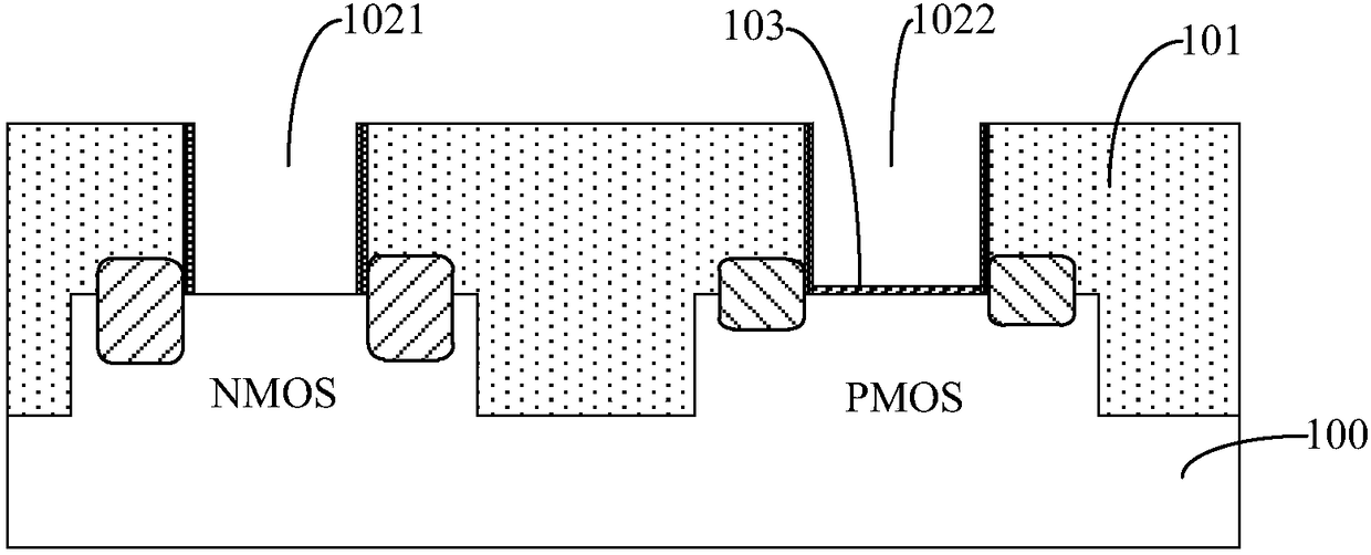
[0048] Step S2, forming a high-k dielectric layer at the bottom of the gate trench, which further includes the following step: before forming the high-k dielectric layer, performing a first anneal in an atmosphere containing hydrogen to passivating dangling bonds in the semiconductor substrate exposed from the gate trenches, and / or, after forming the high-k dielectric layer, performing a second anneal to passivate the high-k dielectric layer Oxygen holes in the electrical layer.
[0049] According to the manufacturing method of the present invention, before forming the high-k dielectric layer, the first annealing is performed in an...
Embodiment 2
[0141] The present invention also provides a semiconductor device, which is prepared by the manufacturing method in the first embodiment above.
[0142] Refer below Figure 1E The structure of the semiconductor device of the present invention will be described in detail. Wherein, in this embodiment, a FinFET device is mainly taken as an example.
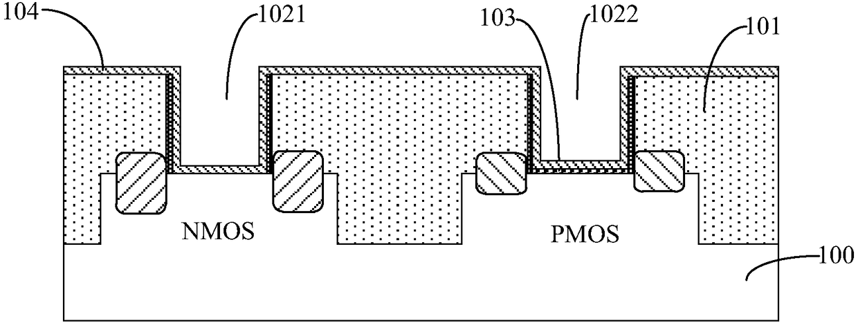
[0143] Specifically, the semiconductor device includes a semiconductor substrate 100, and the semiconductor substrate 100 may be at least one of the materials mentioned below: silicon, silicon on insulator (SOI), stacked silicon on insulator (SSOI), Silicon germanium on insulator (S-SiGeOI), silicon germanium on insulator (SiGeOI) and germanium on insulator (GeOI) are laminated.
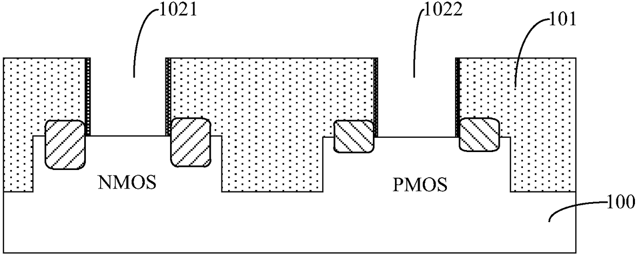
[0144] In one example, the semiconductor substrate includes an NMOS device region and a PMOS device region, wherein a gate trench is formed in the NMOS device region, and a gate trench is formed in the PMOS device region.
[0145] Exemplarily, the channe...
Embodiment 3
[0165] The present invention also provides an electronic device, including the semiconductor device described in Embodiment 2, and the semiconductor device is prepared according to the method described in Embodiment 1.
[0166] The electronic device of this embodiment can be any electronic device such as a mobile phone, a tablet computer, a notebook computer, a netbook, a game console, a TV set, a VCD, a DVD, a navigator, a digital photo frame, a camera, a video camera, a recording pen, MP3, MP4, PSP, etc. Product or equipment, but also any intermediate product including electrical circuits. The electronic device according to the embodiment of the present invention has better performance due to the use of the above-mentioned semiconductor device.
[0167] in, image 3 An example of a mobile phone handset is shown. The mobile phone handset 300 is provided with a display portion 302 included in a housing 301, operation buttons 303, an external connection port 304, a speaker 30...
PUM
| Property | Measurement | Unit |
|---|---|---|
| Thickness | aaaaa | aaaaa |
| Thickness | aaaaa | aaaaa |
| Thickness | aaaaa | aaaaa |
Abstract
Description
Claims
Application Information
 - R&D Engineer
- R&D Manager
- IP Professional
- Industry Leading Data Capabilities
- Powerful AI technology
- Patent DNA Extraction
Browse by: Latest US Patents, China's latest patents, Technical Efficacy Thesaurus, Application Domain, Technology Topic, Popular Technical Reports.
© 2024 PatSnap. All rights reserved.Legal|Privacy policy|Modern Slavery Act Transparency Statement|Sitemap|About US| Contact US: help@patsnap.com