A kind of non-leakage Mesa scribe line 3D through-hole superstructure LED chip and preparation method thereof

A technology of LED chips and dicing lines, applied in circuits, electrical components, semiconductor devices, etc., can solve the problems of substandard appearance yield of dicing line edges, poor appearance of scribing line edges, unstable corrosion process, etc., and achieve excellent super current Driving capability, excellent current expansion capability, stable and easy-to-control process

Active Publication Date: 2019-11-15
SOUTH CHINA UNIV OF TECH
View PDF3 Cites 0 Cited by
  • Summary
  • Abstract
  • Description
  • Claims
  • Application Information

AI Technical Summary

Problems solved by technology

Wet etching has disadvantages such as MESA scribe line white edge, scribe line edge appearance yield rate is not up to standard, scribe line edge corrosion liquid penetrates into semiconductor and metal layer, corrosion process is unstable, difficult to control, etc.; while dry etching can solve the problem of scribe line The edge appearance is poor and the process is unstable, but there are also problems such as metal backsplash caused by plasma overbombing, metal climbing to the side wall of MESA, etc. These problems will lead to different degrees of cutting line leakage. The only way to prepare high-performance, high-yield 3D through-hole superstructure LED chips, and also the only way to realize high-power, super-drive LED lighting technology

Method used


Image

  • A kind of non-leakage Mesa scribe line 3D through-hole superstructure LED chip and preparation method thereof
  • A kind of non-leakage Mesa scribe line 3D through-hole superstructure LED chip and preparation method thereof
  • A kind of non-leakage Mesa scribe line 3D through-hole superstructure LED chip and preparation method thereof

Examples


Embodiment 1

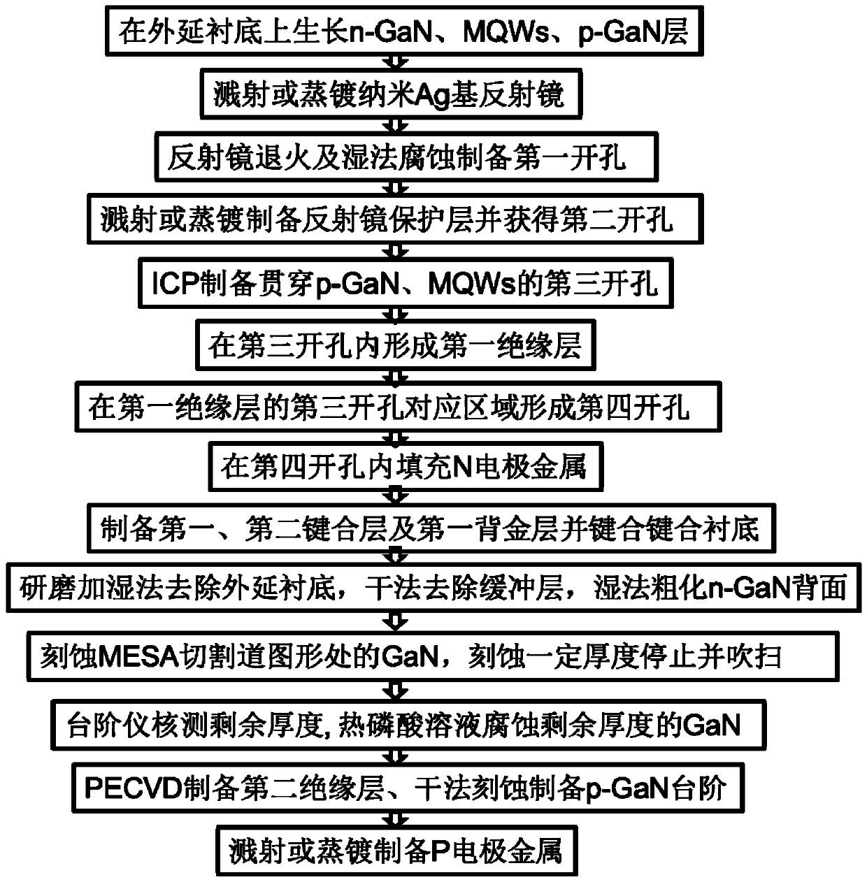
[0049] A method for preparing a no-leakage MESA scribe line 3D through-hole superstructure LED chip, comprising the following preparation steps:

[0050] (1) Provide a silicon substrate, and epitaxially grow LED epitaxial wafers on the silicon substrate, including n-type doped GaN films grown on epitaxial substrates, and InGaN / GaN multiple quantum wells grown on n-type doped GaN films , p-type doped GaN films grown on InGaN / GaN multiple quantum wells. The silicon substrate has a (111) plane as an epitaxial plane. The thickness of the n-type doped GaN film is 2.5um; the InGaN / GaN quantum well is a 12-period InGaN well layer / GaN barrier layer, wherein the thickness of the InGaN well layer is 3nm, and the thickness of the GaN barrier layer is 11nm ; The thickness of the p-type doped GaN film is 300nm;

[0051] (2) Evaporate nano-Ag-based reflectors on the surface of LED epitaxial wafers using electron beam evaporation process. The evaporation rate is 3Å / s, and the evaporation t...

Embodiment 2

[0067] A method for preparing a no-leakage MESA scribe line 3D through-hole superstructure LED chip, comprising the following preparation steps:

[0068](1) Provide GaN substrates, epitaxially grow LED epitaxial wafers on epitaxial substrates, including n-type doped GaN films grown on epitaxial substrates, and InGaN / GaN multiple quantum wells grown on n-type doped GaN films , p-type doped GaN films grown on InGaN / GaN quantum wells. The thickness of the n-type doped GaN film is 3.5um; the InGaN / GaN quantum well is a 6-period InGaN well layer / GaN barrier layer, wherein the thickness of InGaN is 6nm, and the thickness of the GaN barrier layer is 11nm; The thickness of the p-type doped GaN film is 400nm;

[0069] (2) Use magnetron sputtering to sputter nano-Ag-based mirrors on the surface of the LED epitaxial wafer, the sputtering power is 4.5kW, the sputtering rate is 20Å per second, the maximum sputtering temperature is 88°C, and the sputtering pressure is 0.04mbar . The prep...


PUM

PropertyMeasurementUnit
thicknessaaaaaaaaaa
thicknessaaaaaaaaaa
thicknessaaaaaaaaaa

Abstract

The invention discloses an electric-leakage-free LED chip of a 3D through hole superstructure with an MESA cutting channel and a preparation method of the LED chip. The preparation method comprises that an n type doped GaN layer, an InGaN / GaN multi-quantum well layer and a p type doped GaN layer are prepared on an epitaxial substrate, a nanometer Ag-based reflector is prepared in the surface of anLED epitaxial wafer, and a reflector protective layer, MESA holes and an insulating layer are prepared; N metal electrodes and bonding layer metal are filled into the holes; an LED epitaxial layer istransferred to position on a Si substrate; the MESA cutting channel is prepared in a dry and wet combined method; and a passivation layer PA, a P electrode pattern and P electrode metal are preparedto form the LED chip. The thickness ratio etching the MESA cutting channel in the dry and wet method is optimized, the obtained GaN MESA cutting channel is tidy in edge, free of penetration of a corrosion liquid, free of white edges, free of climbing and backwash of the metal sidewall, and stable and easy control in technology, and the problem of electric leakage of the LED chip is solved.

Description

technical field [0001] The invention relates to the field of LED manufacturing, in particular to a no-leakage MESA scribe line 3D through-hole superstructure LED chip and a preparation method thereof. Background technique [0002] With the gradual application of LEDs in the field of lighting, the market has higher and higher requirements for the light efficiency of white LEDs. At present, the GaN-based vertical linear structure LED chips emerging in the LED market, because of their single-sided light output and good heat dissipation capabilities, can withstand A series of advantages such as high current injection and a fraction of the cost of the formal structure are gradually replacing sapphire-based horizontal structure LED chips and becoming the first choice in the high-power LED market. But the vertical linear structure LED also has its disadvantages. First, because its N electrode is placed on the light-emitting surface, there is a serious problem of electrode light blo...

Claims


Application Information

Patent Timeline
Patent Type & Authority Patents(China)
IPC IPC(8): H01L33/48H01L33/00
CPCH01L33/005H01L33/48
Inventor 李国强张云鹏
Owner SOUTH CHINA UNIV OF TECH
Why Eureka
Try Eureka