Local-field-enhancement-type, wide-spectrum and high-response photoelectric detector

A photodetector and wide-spectrum technology, applied in the field of photodetectors, can solve the problems of narrow detection spectrum and low response, and achieve the effects of widening the detection range, improving the response speed, and improving the mobility.

Active Publication Date: 2018-08-10
UNIV OF ELECTRONIC SCI & TECH OF CHINA
View PDF4 Cites 1 Cited by
  • Summary
  • Abstract
  • Description
  • Claims
  • Application Information

AI Technical Summary

Problems solved by technology

[0004] The object of the present invention is: the present invention provides a photodetector with local field enhancement type wide spectrum and high response, which solves the problem that the material absorption of existing photodetectors is limited by the enhanced material, and the energy level of the material is fixed after contact with graphene Only forward injection or reverse injection can be realized, which leads to the problem of narrow detection spectrum and low response

Method used


Image

  • Local-field-enhancement-type, wide-spectrum and high-response photoelectric detector
  • Local-field-enhancement-type, wide-spectrum and high-response photoelectric detector
  • Local-field-enhancement-type, wide-spectrum and high-response photoelectric detector

Examples


Embodiment 1

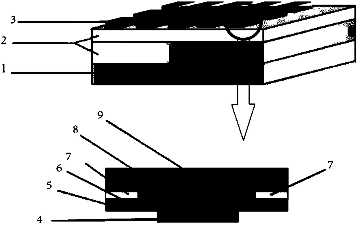
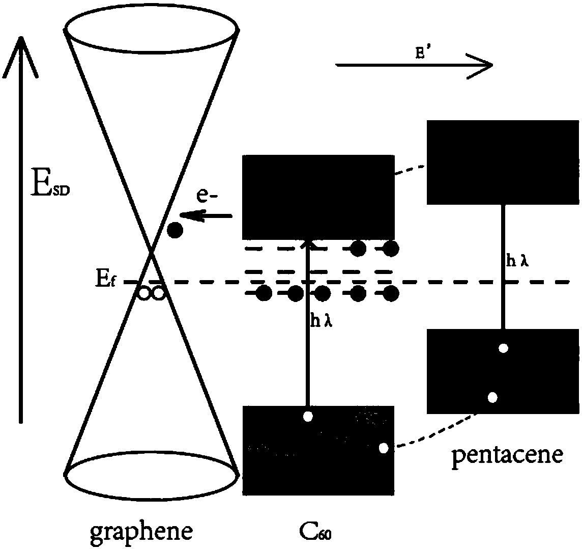
[0034] The thickness of the fullerene film 8 is 1.0nm, the material is C60, the P-type organic semiconductor film 9 is pentacene, the substrate is a silicon wafer with a readout circuit, the surface is covered with a silicon nitride dielectric layer and the electrical interface of the detection unit , The short-wave band of this device includes visible light, and the long-wave band includes near-infrared; when receiving the short-wave band, C60 and pentacene form an enhanced layer to absorb light radiation and generate electron-hole pairs. After the electron-hole pairs are separated, electrons are injected into graphene6 , The holes are bound to pentacene, causing the conduction channel resistance to change to improve the light response; when receiving long-wavelength bands, graphene 6 is the light absorption layer, and the energy level transition between graphene 6 and C60 causes the reverse injection of electrons, The electrons recombine with the holes of pentacene to amplify ...

Embodiment 2

[0036] The thickness of the fullerene film 8 ranges from 0.5 to 15 nm. The thickness is selected according to the actual situation. The appropriate thickness determines the strength of the fullerene material's ability to absorb electrons. The positions of electron-hole pairs are different in different wavebands. The electrons generated in the short wave band are injected into graphene 6, and the long wave band is in graphene 6. Electron-hole pairs are generated in the EMI and injected into the fullerene film 8 to cause a change in resistance and achieve high response in different wavelength bands.

Embodiment 3

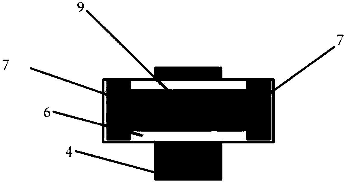
[0038] The graphene 6 is connected to the metal source electrode and the metal drain electrode on the dielectric layer 5, and the conductive channel of the detector is formed after the metal source electrode and the metal drain electrode are applied with the working voltage; the short wave band of this device includes visible light, and the long wave band includes near Infrared, the carrier transport mechanism of visible light and near-infrared are different: when visible light is irradiated on the device, the enhancement layer absorbs and generates photo-generated electron-hole pairs, which diffuse to the interface of the two materials, built-in Under the action of the electric field, the electron-hole pairs are effectively separated, the electrons enter the N-type acceptor fullerene film 8, and the holes are trapped in the P-type organic semiconductor film 9. The electrons accumulated in the fullerene film 8 are The concentration difference between the graphene 6 and the fulle...


PUM

PropertyMeasurementUnit
Thicknessaaaaaaaaaa
Thicknessaaaaaaaaaa

Abstract

The present invention discloses a local-field-enhancement-type, wide-spectrum and high-response photoelectric detector, pertaining to the field of the photoelectric detectors. The detector comprises asilicon substrate, an IC circuit and a detector unit array arranged from bottom to top. The detector unit array comprises, arranged from bottom to top, a field effect transistor unit used for changing detection range(s) and providing conducting channel(s) and an enhanced absorption unit used for separating photo-generated electrons and holes after a donor-receptor local electric field is formed.The detector unit array is used for forward injection in a short-wave band and reverse injection in a long-wave band of detection signal current(s) capable of realizing wide-spectrum and high-response. According to the detector, the problems of the conventional photoelectric detector, for example, the light absorption of the material of the conventional photoelectric detector is limited by a reinforced material, and the energy level is fixed after the material contacts with graphene, so that the material can only realize forward injection or reverse injection, resulting in narrow detection spectrum and low response, are solved. The photoelectric detector can realize the detection effects of wide-spectrum and high-response in the visible light band and the near infrared band.

Description

Technical field [0001] The invention relates to the field of photodetectors, in particular to a photodetector with local field enhancement type wide spectrum and high response. Background technique [0002] The two-dimensional Dirac material graphene and the three-dimensional Vidillac material cadmium arsenide have attracted widespread attention due to their extraordinary electronic and optical properties, and they have great potential in photoelectric applications such as photodetection. Graphene is a single-atom layered two-dimensional Dirac semi-metal material. The carbon atoms are arranged in a hexagonal honeycomb lattice and have many electronic, optical, mechanical and thermal properties. The electrons transferred in graphene appear as massless Dirac fermions, and the relationship between energy and momentum is linear, which makes the charge carrier mobility of graphene reach 10 at room temperature. 5 cm 2 / Vs, reach 10 at low temperature 6 cm 2 / Vs. This excellent electro...

Claims


Application Information

Patent Timeline
IPC IPC(8): H01L27/28H01L27/30H01L51/42
CPCH10K19/201H10K19/20H10K39/30H10K19/10H10K30/354H10K2102/00Y02E10/549
Inventor 王军韩嘉悦刘鹏田夫兰杨明
Owner UNIV OF ELECTRONIC SCI & TECH OF CHINA
Why Eureka
Try Eureka