A kind of opposite-side cascade semiconductor chip device and cascade method

A semiconductor and chip-level technology, applied in semiconductor devices, semiconductor/solid-state device manufacturing, semiconductor/solid-state device components, etc., to achieve high surface activity and surface energy, save packaging space, and prevent pollution

Active Publication Date: 2020-04-21
CHENGDU HIWAFER SEMICON CO LTD
View PDF4 Cites 0 Cited by
  • Summary
  • Abstract
  • Description
  • Claims
  • Application Information

AI Technical Summary

Problems solved by technology

[0007] The purpose of the present invention is to overcome the deficiencies of the prior art, provide a device and cascade method for cascading semiconductor chips on the opposite side, and solve the problem of introducing bond lines in the prior art

Method used


Image

  • A kind of opposite-side cascade semiconductor chip device and cascade method
  • A kind of opposite-side cascade semiconductor chip device and cascade method
  • A kind of opposite-side cascade semiconductor chip device and cascade method

Examples


Embodiment Construction

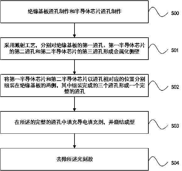
[0043] Further describe the technical scheme of the present invention in detail below in conjunction with accompanying drawing:

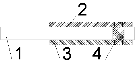
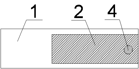
[0044] Such as figure 1 and figure 2 Shown, a kind of opposite-side cascaded semiconductor chip device comprises:

[0045] An insulating substrate 1, the insulating substrate 1 has a first through hole 5;

[0046] The first semiconductor chip 2 and the second semiconductor chip 3 assembled on both sides of the insulating substrate 1 respectively; wherein, the first semiconductor chip 2 has a second through hole 7, and the second semiconductor chip 3 has a third through hole 8, after the assembly is completed After the first through hole 5, the second through hole 7 and the third through hole 8 form a complete through hole 9; the first through hole 5, the second through hole 7 and the third through hole 8 all have metallization side wall;

[0047] The conductive filler 4 filled to the complete through hole 9 and sintered into shape.

[0048] In...


PUM


Abstract

The invention discloses an opposite-side cascade semiconductor chip device and a cascade method. The device comprises an insulation substrate having a first through hole, and a first semiconductor chip and a second semiconductor chip respectively assembled at two sides of the insulation substrate, wherein the first semiconductor chip has a second through hole, the second semiconductor chip has a third through hole, after assembling, the first through hole, the second through hole and the third through hole form an integral through hole, the first through hole, the second through hole and the third through hole respectively have a metalized side wall, filling to the integral through hole is carried out, and sintering of a molded conductive filler is carried out. The device is advantaged inthat the semiconductor process is employed, through processing the metalized side wall and corresponding position assembling, the conductive filler is filled in the through hole, cascading the two chips on both sides of the same substrate is realized, the packaging space is effectively saved, and the risk of bond line introduction can be effectively avoided.

Description

technical field [0001] The invention relates to the field of semiconductor manufacturing, in particular to an opposite-side cascaded semiconductor chip device and a cascaded method. Background technique [0002] With the continuous advancement of science and technology, people's needs are increasing day by day, and the requirements for semiconductor chips are getting higher and higher. At the same time, with the improvement of people's needs, although the structure, function, and integration of a single chip are becoming more and more complex, but limited by factors such as materials and basic physical theories, it often requires multiple chips of different types and functions to be cascaded, such as At present, the widely used RF front-end chips need cascading of multiple chips such as switch chips, power amplifier chips, and low-noise chips. [0003] At present, microwave radio frequency chips are mostly cascaded in the form of metal bond lines (bonding lines), which have...

Claims


Application Information

Patent Timeline
Patent Type & Authority Patents(China)
IPC IPC(8): H01L23/538H01L21/60
CPCH01L23/5384H01L24/89
Inventor 陈一峰
Owner CHENGDU HIWAFER SEMICON CO LTD
Why Eureka
Try Eureka