Planar cascaded semiconductor chip device and cascaded method

A semiconductor and chip-level technology, applied in semiconductor devices, semiconductor/solid-state device manufacturing, semiconductor/solid-state device components, etc., to achieve high surface activity and surface energy, high precision, and prevent pollution

Active Publication Date: 2020-03-17
CHENGDU HIWAFER SEMICON CO LTD
View PDF7 Cites 0 Cited by
  • Summary
  • Abstract
  • Description
  • Claims
  • Application Information

AI Technical Summary

Problems solved by technology

[0007] The purpose of the present invention is to overcome the deficiencies of the prior art, provide a planar cascaded semiconductor chip device and cascading method, and solve the problem of introducing bond lines in the prior art

Method used


Image

  • Planar cascaded semiconductor chip device and cascaded method
  • Planar cascaded semiconductor chip device and cascaded method
  • Planar cascaded semiconductor chip device and cascaded method

Examples


Embodiment Construction

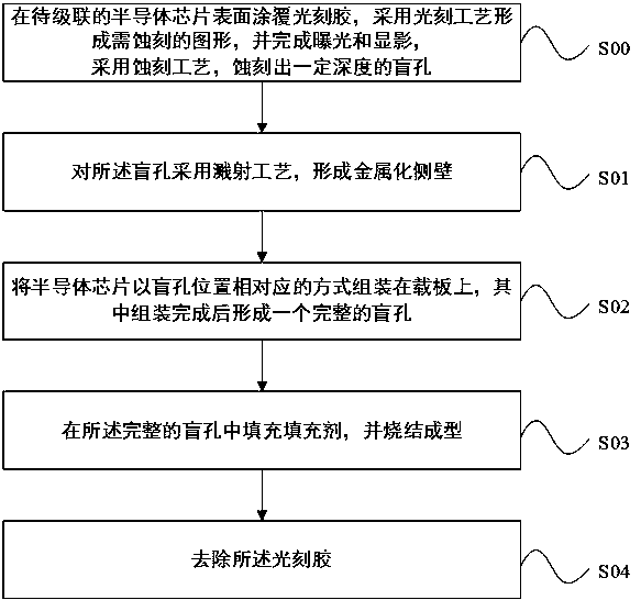
[0040] Further describe the technical scheme of the present invention in detail below in conjunction with accompanying drawing:

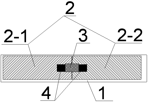
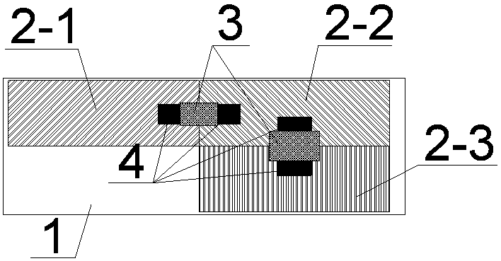
[0041] Such as figure 1 and figure 2 As shown, a planar cascaded semiconductor chip device includes:

[0042] Carrier 1;

[0043] At least two semiconductor chips 2 assembled on the same plane of the carrier plate 1; wherein, each semiconductor chip 2 has at least one blind hole 6, and the positions of the blind holes 6 of the two semiconductor chips 2 correspond to form a complete The blind hole 6; the blind hole 6 includes a metallized side wall;

[0044] The conductive filler 3 filled to the complete blind hole 6 and sintered.

[0045] specifically, figure 1 Shown this device to comprise the embodiment 1 of two semiconductor chips 2, described device comprises:

[0046] Carrier 1;

[0047] The first semiconductor chip 2-1 and the second semiconductor chip 2-2 assembled on the same plane of the carrier plate 1; wherein, in this embodiment,...


PUM


Abstract

The invention discloses a plane cascading semiconductor chip device and a cascading method. The device comprises a supporting plate, at least two semiconductor chips assembled on the same plane of thesupporting plate, wherein each semiconductor chip is provided with at least one blind hole, after assembling is completed, and the blind holes in the two semiconductor chip correspondingly form one complete blind hole; the complete blind hole includes a metal side wall; the complete blind hole is filled with a conductive filling agent which is sintered and molded. By adopting the semiconductor technology, the blind hole of the certain depth is formed at the place needing cascading of the two chips, in the follow-up machining process, the blind hole is filled with nano-silver, cascading planarization of the whole chip is achieved, and the risk caused by introducing a bond wire is effectively avoided.

Description

technical field [0001] The invention relates to the field of semiconductor manufacturing, in particular to a planar cascaded semiconductor chip device and a cascaded method. Background technique [0002] With the continuous advancement of science and technology, people's needs are increasing day by day, and the requirements for semiconductor chips are getting higher and higher. At the same time, with the improvement of people's needs, although the structure, function, and integration of a single chip are becoming more and more complex, but limited by factors such as materials and basic physical theories, it often requires multiple chips of different types and functions to be cascaded, such as At present, the widely used RF front-end chips need cascading of multiple chips such as switch chips, power amplifier chips, and low-noise chips. [0003] At present, microwave radio frequency chips are mostly cascaded in the form of metal bond wires (bonding wires), which has many dis...

Claims


Application Information

Patent Timeline
Patent Type & Authority Patents(China)
IPC IPC(8): H01L23/13H01L23/488H01L21/033H01L21/60
CPCH01L21/0334H01L23/13H01L23/488H01L24/63
Inventor 陈一峰
Owner CHENGDU HIWAFER SEMICON CO LTD
Why Eureka
Try Eureka