Storage unit of resistive random access memory (RRAM), manufacturing method of storage unit and electronic device
A random access memory and memory cell technology, applied in circuits, electrical components, semiconductor devices, etc., can solve problems such as working life, insufficient read and write speed, high voltage and size that cannot continue to shrink the development of flash memory, etc., to improve durability and Window range, effect of high storage density
- Summary
- Abstract
- Description
- Claims
- Application Information
AI Technical Summary
Problems solved by technology
Method used
Image


Examples
Embodiment 1
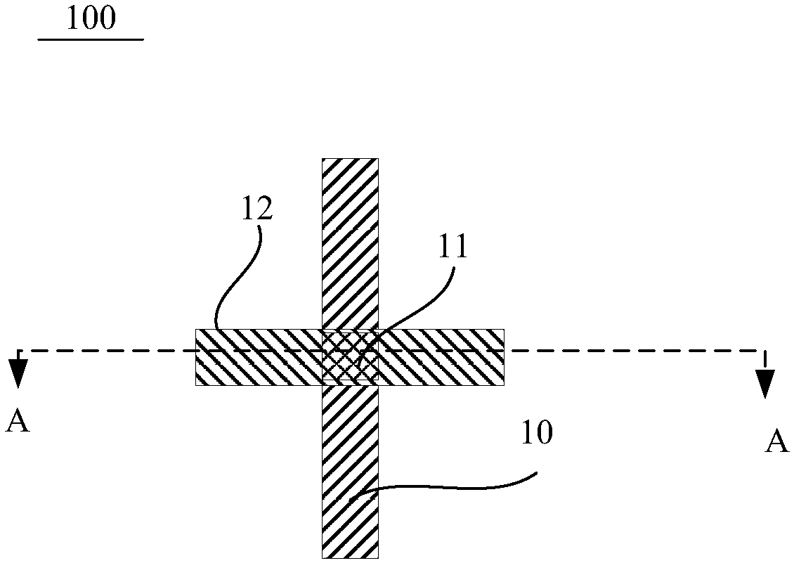
[0044] The following will refer to Figure 3A ~ Figure 7A , Figure 3B to Figure 7B The manufacturing method of the RRAM storage unit according to an embodiment of the present invention is described in detail. Figure 3A ~ Figure 7A It shows a schematic cross-sectional view of the device obtained by sequentially implementing each step of the manufacturing method of the resistive random access memory unit according to an embodiment of the present invention; Figure 3B ~ Figure 7B It shows a schematic top view of a semiconductor device obtained by sequentially implementing each step of a manufacturing method of a resistive random access memory unit according to an embodiment of the present invention, Figure 3B ~ Figure 7B Followed by Figure 3A ~ Figure 7A Sectional view along B-B direction. In this embodiment, taking a resistive random access memory cell (3D CBRAM) with a conductive bridge structure as an example, the method for manufacturing the resistive random access mem...
Embodiment 2
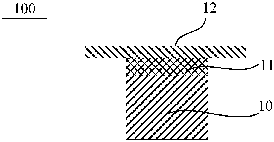
[0066] This embodiment proposes a resistive random access memory storage unit, such as Figure 7A and Figure 7B As shown, the resistive random access memory unit includes a semiconductor substrate 300, on which a stacked structure is formed, and the stacked structure includes first electrode layers 301 and isolation layers 302 stacked alternately. A resistive variable layer is formed on the sidewall of the stacked structure, and at least the second electrode layer 305A is formed on the sidewall of the resistive variable layer.
[0067] In an example of the present invention, the resistive random access memory unit is formed using a conductive bridging mechanism, and the first electrode layer 301 can use various metal or alloy electrode materials. Exemplarily, in this embodiment, the first electrode Layer 301 is platinum, tungsten, copper, silver or titanium nitride. The second electrode layer 305A can be made of various suitable metals or alloy materials, such as suitable m...
Embodiment 3
[0075] Another embodiment of the present invention provides an electronic device, including the above RRAM storage unit and electronic components connected to the RRAM storage unit. Wherein, the resistive random access memory unit includes: a semiconductor substrate, on which a stacked structure is formed, and the stacked structure includes first electrode layers and isolation layers stacked alternately; on the side of the stacked structure A resistive switch layer is formed on the wall; a second electrode layer is formed at least on the side wall of the resistive switch layer.
[0076] Wherein, the semiconductor substrate can be at least one of the materials mentioned below: Si, Ge, SiGe, SiC, SiGeC, InAs, GaAs, InP or other III / V compound semiconductors, including multilayers composed of these semiconductors The structure or the like may be silicon-on-insulator (SOI), silicon-on-insulator (SSOI), silicon-germanium-on-insulator (S-SiGeOI), silicon-germanium-on-insulator (SiGe...
PUM
 Abstract
Description
Claims
Application Information
 - R&D
- Intellectual Property
- Life Sciences
- Materials
- Tech Scout
- Unparalleled Data Quality
- Higher Quality Content
- 60% Fewer Hallucinations
Browse by: Latest US Patents, China's latest patents, Technical Efficacy Thesaurus, Application Domain, Technology Topic, Popular Technical Reports.
© 2025 PatSnap. All rights reserved.Legal|Privacy policy|Modern Slavery Act Transparency Statement|Sitemap|About US| Contact US: help@patsnap.com