
LED packaging structure and packaging method

A technology of LED packaging and LED chips, applied in electrical components, circuits, semiconductor devices, etc., can solve problems such as UV radiation resistance, high temperature resistance, and inconvenience in industrialization, and achieve improved luminous efficiency, fast heat dissipation, and consistent paths. Effect

Inactive Publication Date: 2018-07-10
SHENZHEN GUANGMAO ELECTRONICS
View PDF12 Cites 0 Cited by
  • Summary
  • Abstract
  • Description
  • Claims
  • Application Information

AI Technical Summary

Problems solved by technology

[0004] At present, the commonly used LED packages have slow heat dissipation, are not resistant to UV radiation, are not resistant to high temperature, are easy to turn yellow, and are not convenient for industrialization.

Method used


Image

  • LED packaging structure and packaging method
  • LED packaging structure and packaging method
  • LED packaging structure and packaging method

Examples


Embodiment Construction

[0040] In order to facilitate the understanding of the present invention, the present invention will be described more fully below with reference to the associated drawings. Preferred embodiments of the invention are shown in the accompanying drawings. However, the present invention can be embodied in many different forms and is not limited to the embodiments described herein. On the contrary, the purpose of providing these embodiments is to make the disclosure of the present invention more thorough and comprehensive.

[0041] Unless otherwise defined, all technical and scientific terms used herein have the same meaning as commonly understood by one of ordinary skill in the technical field of the invention. The terminology used herein in the description of the present invention is only for the purpose of describing specific embodiments, and is not intended to limit the present invention. As used herein, the term "and / or" includes any and all combinations of one or more of th...


PUM


Abstract

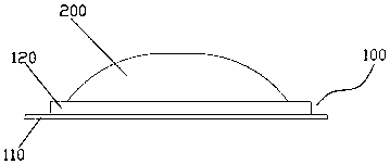
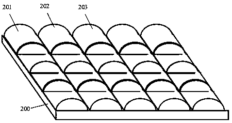
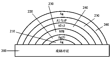
The invention discloses an LED packaging structure. The LED packaging structure comprises a packaging main body; the packaging main body comprises a substrate and a Kovar alloy metal frame arranged above the substrate; a conductive layer is arranged on the Kovar alloy metal frame; a die bonding region is arranged on the conductive layer; the die bonding region is used for mounting an LED chip; a glass substrate is mounted on the die bonding region; the periphery of the glass substrate is covered with a protection cover; the outer surface of the glass cover is of a convex-convex structure; an edge filter and diffuser are also included in the packaging main body; and the diffuser is used for receiving light reflected from the edge filter. By virtue of the packaging structure, the LED can bequick in heat dissipation, resistant to UV radiation, resistant to high temperature, resistant to yellowing change and convenient in realization of industrialization; the excited light ray paths of the light can be consistent, so that there is no color difference or little color difference seen from each angle; the light rays emitted from the LED chip can be reflected through the conductive layerto form a reflection layer; and the protection cover adopts the concave-convex structure, so that roughening of the LED packaging body surface can be realized effectively and simply, thereby improvingthe light emitting efficiency of the efficient LED.

Description

technical field [0001] The invention relates to the field of semiconductor packaging, in particular to an LED packaging structure and a packaging method thereof. Background technique [0002] LED is called the fourth-generation lighting source or green light source. It has the characteristics of energy saving, environmental protection, long life, and small size. It is widely used in various indications, displays, decorations, backlights, general lighting, and urban night scenes. According to different functions, it can be divided into five categories: information display, signal lights, vehicle lamps, LCD backlight, and general lighting. [0003] LED products are mainly used in the three major fields of backlight, color screen and indoor lighting. In the future, under the influence of factors such as the decline in product prices caused by the continuous maturity of technology and the rise of a new round of global ban on the sale of incandescent lamps, indoor lighting will ...

Claims


Application Information

Patent Timeline
Patent Type & Authority Applications(China)
IPC IPC(8): H01L33/48H01L33/60H01L33/62
CPCH01L33/486H01L33/60H01L33/62H01L2933/0033H01L2933/0066
Inventor 叶浩文李锋
Owner SHENZHEN GUANGMAO ELECTRONICS
Learn More