Active component substrate and manufacturing method thereof

A technology of active components and manufacturing methods, applied in semiconductor/solid-state device manufacturing, electrical components, electrical solid-state devices, etc., can solve the problems of coating thin photoresist materials with stable and difficult control, large variation, and difficult mass production, etc. Achieve the effects of small channel size variation, consistent electrical characteristics, and high mass production

Active Publication Date: 2018-06-29
AU OPTRONICS CORP
View PDF5 Cites 0 Cited by
  • Summary
  • Abstract
  • Description
  • Claims
  • Application Information

AI Technical Summary

Problems solved by technology

The bottom angle of the protrusion and the stability of the process of coating thin photoresist materials are not easy to control, resulting in large variations in multiple channels of multiple thin film transistors formed on the same substrate (that is, electrical characteristics, such as: turn-on current, large variation), mass production is not easy

Method used


Image

  • Active component substrate and manufacturing method thereof
  • Active component substrate and manufacturing method thereof
  • Active component substrate and manufacturing method thereof

Examples


Embodiment Construction

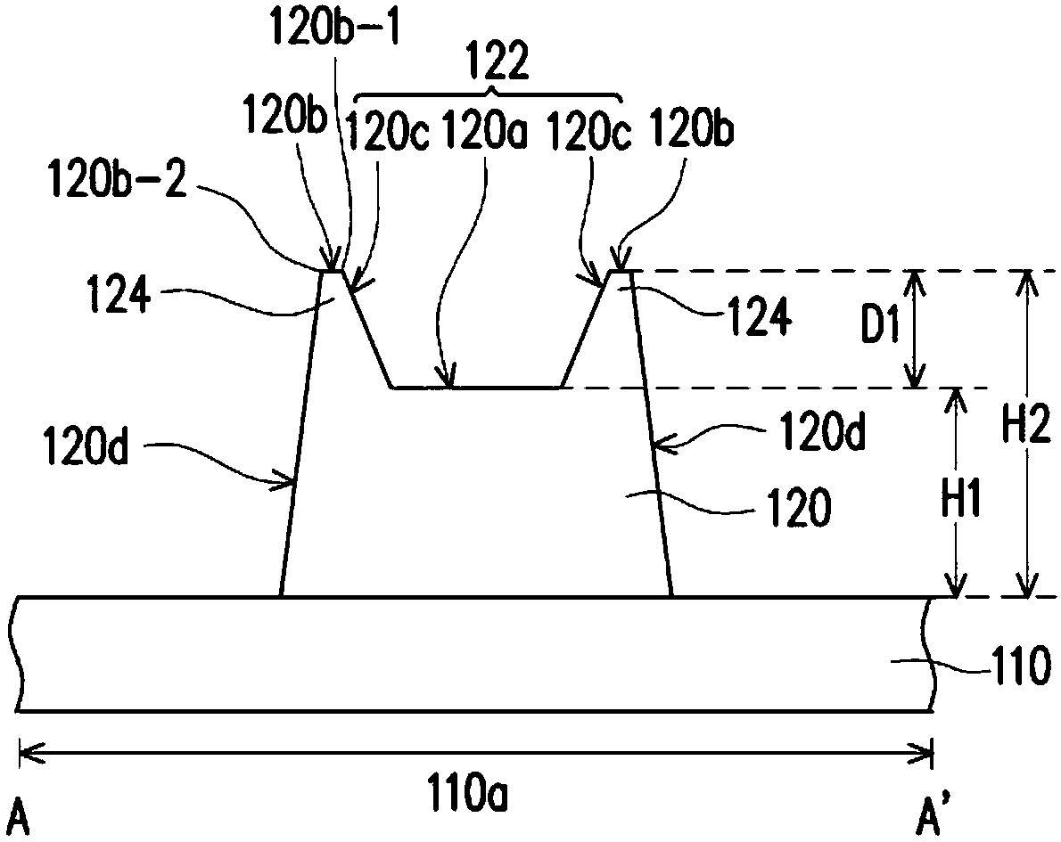
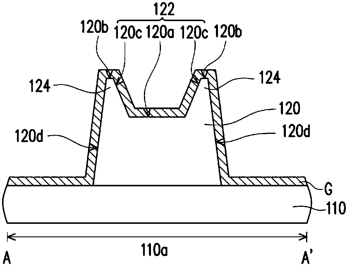
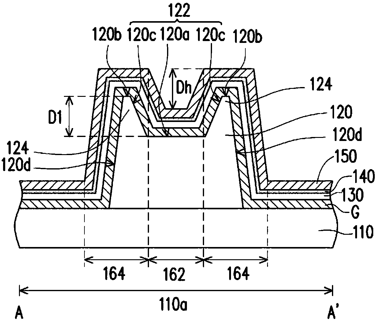
[0066] Figure 1A to Figure 1I It is a schematic cross-sectional view of the manufacturing process of the active device substrate according to an embodiment of the present invention. Figure 2A It is a schematic top view of an active device substrate according to an embodiment of the present invention. Figure 2B for Figure 2A An enlarged schematic view of part of the display area of ​​the active device substrate. especially, Figure 1I corresponds to Figure 2B The section line A-A' of , and Figure 2B The illustration of the common electrode 194 is omitted.

[0067] Please refer to Figure 1A , firstly, a substrate 110 is provided. In this embodiment, the substrate 110 may have a display area 110a and a peripheral area 110b outside the display area 110a (marked in Figure 2A ). In this embodiment, the material of the substrate 110 can be glass, quartz, organic polymer, or opaque / reflective material (for example: conductive material, metal, wafer, ceramic, or other a...


PUM


Abstract

An active component substrate includes a substrate and an active component. The active device includes a bump, a gate on the bump, a semiconductor layer, a gate insulating layer between the gate and the semiconductor layer, and first and second electrodes electrically connected to the semiconductor layer. The bump has a first upper surface, a second upper surface, an inner side surface, and an outer side surface. The distance between the second upper surface and the substrate is greater than the distance between the first upper surface and the substrate. The inner side defines a recess with the first upper surface. The inner side surface, the second upper surface, and the outer side surface define a convex portion. The semiconductor layer is located on the first upper surface, the inner side surface, the second upper surface, and the outer side surface. The first electrode is located on at least a portion of the outer side. The second electrode is located in the recess of the bump. Thebump separates the first electrode from the second electrode. Further, a method of manufacturing the active component substrate is also provided.

Description

technical field [0001] The invention relates to an element substrate and a manufacturing method thereof, and in particular to an active element substrate and a manufacturing method thereof. Background technique [0002] Among many flat-panel displays, Thin Film Transistor Liquid Crystal Display (TFT-LCD) has superior characteristics such as high space utilization efficiency, low power consumption, no radiation and low electromagnetic interference. Therefore, LCD displays are very popular among consumers. . The thin film transistor liquid crystal display is mainly composed of an active array substrate, a color filter substrate and a liquid crystal layer between the two substrates. The active array substrate has a display area and a peripheral area. The active array is located in the display area, and the driving circuit is located in the peripheral area. [0003] Taking the active array on the active area as an example, thin film transistors with a high ratio of channel wi...

Claims


Application Information

Patent Timeline
Patent Type & Authority Applications(China)
IPC IPC(8): H01L27/12H01L21/77
CPCH01L27/1214H01L27/1222H01L27/1296G02F1/1368H01L27/1218H01L27/124H01L27/1262H01L27/1288H01L29/41733H01L29/42384H01L29/78603H01L29/78696
Inventor 张吉和
Owner AU OPTRONICS CORP
Why Eureka
Try Eureka