Array substrate, manufacturing method thereof, and display device

A technology for array substrates and manufacturing methods, applied in the display field, can solve problems such as electrical degradation of flexible substrates, and achieve the effect of saving laser resources and scanning time

Active Publication Date: 2020-12-18
BOE TECH GRP CO LTD
View PDF8 Cites 0 Cited by
  • Summary
  • Abstract
  • Description
  • Claims
  • Application Information

AI Technical Summary

Problems solved by technology

[0004] The purpose of the present invention is to provide an array substrate and its manufacturing method, a display panel and a display device. The display area adopts an organic thin film transistor to solve the problems that the existing flexible substrate can only be partially bent and the electrical degradation after bending.

Method used


Image

  • Array substrate, manufacturing method thereof, and display device
  • Array substrate, manufacturing method thereof, and display device
  • Array substrate, manufacturing method thereof, and display device

Examples


Embodiment Construction

[0033] The present invention will be further described below with reference to the accompanying drawings and exemplary embodiments, wherein the same reference numerals in the accompanying drawings all refer to the same components. Also, detailed descriptions of known arts will be omitted if they are unnecessary to illustrate the features of the present invention.

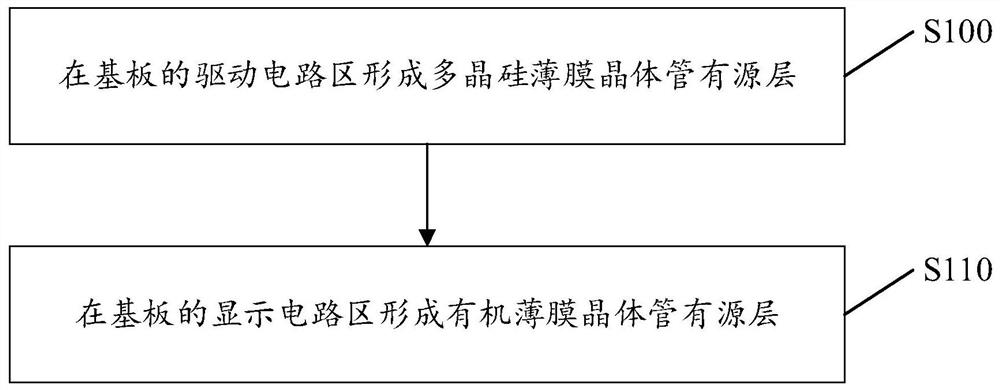
[0034] The present invention firstly provides a method for manufacturing an array substrate, the flow chart of which is shown in figure 2 shown, including the following steps:

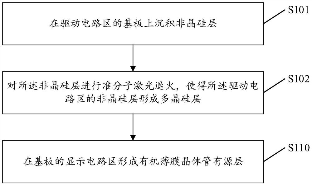
[0035] S100, forming an active layer of a polysilicon thin film transistor in the driving circuit area of ​​the substrate;

[0036] Polysilicon thin film transistors are used in the driving circuit area, and the figure 1 or Figure 4 In the figure about the composition area of ​​the display panel, it is understood that the driving circuit area includes the source driving circuit area 101 and the GOA driving circuit area 102, and polysili...


PUM


Abstract

The present invention relates to the technical field of display, especially to an array substrate and a preparation method thereof, and a display device. The preparation method of the array substratecomprises the steps of: forming an active layer of a polycrystalline silicon thin film transistor at a drive circuit area of a substrate; and forming an active layer of an organic thin film transistorat a display circuit area of the substrate. The array substrate and the preparation method thereof, and the display device employ preparation of the organic thin film transistor at the display circuit area, the organic thin film transistor can still keep good dynamic display after being bent for many times, and therefore, the yield of the display is improved and the production cost is reduced.

Description

【Technical field】 [0001] The present invention relates to the field of display technology, in particular to an array substrate, a manufacturing method thereof, and a display device. 【Background technique】 [0002] At present, commonly used active-matrix liquid crystal displays mostly use amorphous silicon thin film transistors and polysilicon thin film transistors. Among them, the polysilicon thin film transistor (Thin Film Transistor, referred to as TFT) has the advantages of high resolution, fast response, high brightness, high aperture ratio, etc., and the silicon crystal arrangement of the polysilicon thin film transistor is more orderly than that of amorphous silicon, making the polysilicon thin film The transistor has a high electron mobility, and the peripheral driving circuit can be fabricated on the glass substrate at the same time, so as to achieve the goal of system integration and save space and the cost of the driving IC. [0003] However, at present, when maki...

Claims


Application Information

Patent Timeline
Patent Type & Authority Patents(China)
IPC IPC(8): H01L21/84H01L27/12
CPCH01L27/1225H01L27/1229H01L27/127
Inventor 田雪雁刘政
Owner BOE TECH GRP CO LTD
Why Eureka
Try Eureka