Semiconductor package structure with pin sidewall tin climbing function and its manufacturing process

A technology of packaging structure and manufacturing process, applied in the direction of semiconductor/solid-state device manufacturing, semiconductor devices, semiconductor/solid-state device components, etc., can solve the problems of product failure, delamination, difficult to form, etc., to improve the reliability of welding , The effect of improving welding performance and saving equipment cost

Active Publication Date: 2020-06-09
JCET GROUP CO LTD
View PDF12 Cites 0 Cited by
  • Summary
  • Abstract
  • Description
  • Claims
  • Application Information

AI Technical Summary

Problems solved by technology

[0009] However, this kind of packaging structure that forms L-shaped outer leads or C-shaped outer leads by cutting ribs also has the following defects when forming L-shaped outer leads or C-shaped outer leads: first, the outer When the pins are formed, the outer pins are bent toward the side of the plastic package, Figure 1G and Figure 1H The inner pin at A will be affected by the rebound force of the metal, which will cause the metal pin to have the stress of being pushed away from the plastic package downwards, and in the case of this downward force, it is easy to cause A. Delamination occurs between the upper surface of the inner pin and the lower surface of the molding compound
In severe cases, it may even lead to an open circuit between the bonding wire at A and the inner pins, resulting in product failure; secondly, when the outer pins are molded in this kind of L-shaped outer pins or C-shaped outer pins package structure , the outer pins are bent towards the side of the plastic package by inserting the forming mold between the outer pins and the plastic package and then bending and forming. Since the metal pins have a certain elastic coefficient, the outer pins will be back when they are stressed. spring relationship, causing the outer pins to form as Figure 1J Form a larger flared opening as in B in , but it is difficult to form a Figure 1G In the shape of vertically sticking to the side of the plastic package; finally, this kind of L-shaped outer lead or C-shaped outer lead packaging structure has a larger volume, because the outer lead is bent to form an L-shaped outer lead or a C-shaped outer lead. Compared with the traditional inner lead package, the external pin package structure has a wider package width, which is not conducive to the development trend of miniaturized packages.

Method used


Image

  • Semiconductor package structure with pin sidewall tin climbing function and its manufacturing process
  • Semiconductor package structure with pin sidewall tin climbing function and its manufacturing process
  • Semiconductor package structure with pin sidewall tin climbing function and its manufacturing process

Examples


Embodiment Construction

[0060] The present invention will be further described in detail below in conjunction with the accompanying drawings and embodiments.

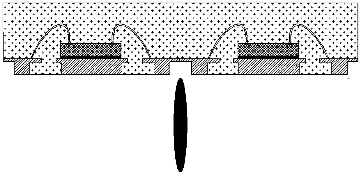
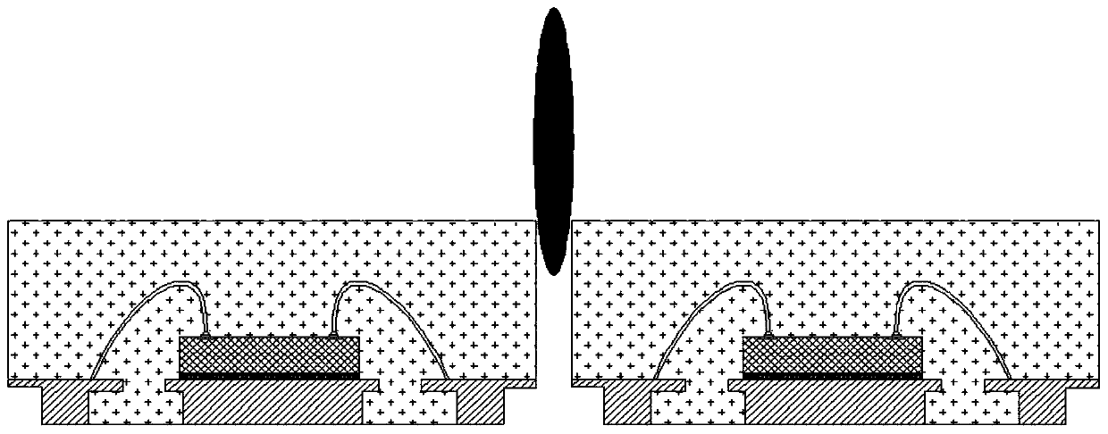
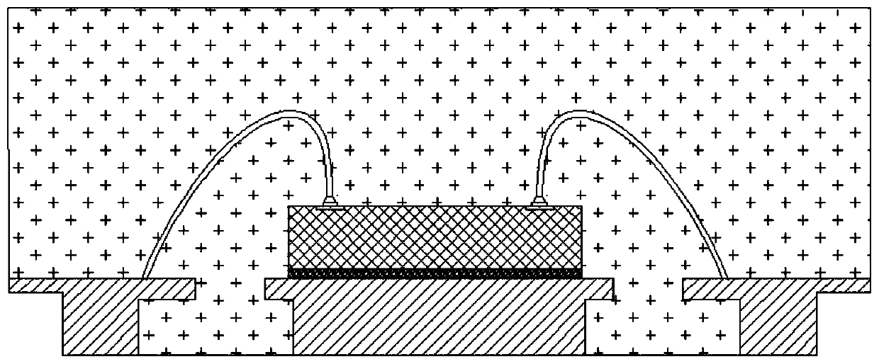
[0061] like figure 2 , image 3 As shown, in this embodiment, a semiconductor package structure with the function of tin climbing on the side wall of the pin includes a base island 1 and a pin 2, the pin 2 is a metal circuit layer formed by electroplating, and the base island 1 is composed of a copper sheet 1.2 and an insulating layer 1.1, the insulating layer 1.1 is located at the bottom of the copper sheet 1.2, the pin 2 is arranged around the base island 3, the pin 2 includes a plane part 2.1 and a side wall part 2.3, the The side wall part 2.3 is located outside the plane part 2.1, and the plane part 2.1 and the side wall part 2.3 are connected by a smooth transition through the arc part 2.2, and the convex surface of the arc part 2.2 faces the outer lower side, and the base island 1 The front side is provided with a chip 4 through an a...


PUM


Abstract

The invention relates to a semiconductor package structure having a pin side wall tin climbing function and a manufacturing process thereof. The structure comprises a paddle and pins, wherein each pincomprises a planar part and a side wall part, the side wall part is arranged at an outer side of the planar part, the planar part and the side wall part are in smooth and transition connection by anarc part, a convex surface of the arc part faces an outer lower side, a chip is arranged on a front surface of the paddle, the chip and the pins form electrical connection by metal welding lines, a plastic sealing material wraps peripheral regions of the paddle, the pins and the chip, and outer surfaces of the planar parts, the arc parts and the side wall parts are exposed out of the plastic sealing material. Welding tin can climb to a relatively high height along the vertical side walls during welding of a PCB, so that the bonding area of the welding tin and the pins is expanded; and meanwhile, air at the pins can be discharged along protruding arcs, so that the welding performance and the welding reliability of a product are improved, and a welding state is intuitively checked.

Description

technical field [0001] The invention relates to a semiconductor packaging structure with the function of tin climbing on the side wall of a pin and a manufacturing process thereof, belonging to the technical field of semiconductor packaging. Background technique [0002] With the development of modern technology, semiconductor packaging has been widely used. Its extensive applications in radar, remote control telemetry, aerospace, etc. put forward higher and higher requirements for its reliability. The failure caused by poor soldering of semiconductors has attracted more and more attention, because this failure is often fatal and irreversible. Therefore, it is very important to get a good soldering reliability in the semiconductor industry. The tin layer on the soldering surface of the semiconductor can make the soldering stronger, especially for automotive electronics. [0003] As we all know, QFN (Quad Flat No-lead Package, four-sided leadless flat package) and DFN (Duad...

Claims


Application Information

Patent Timeline
Patent Type & Authority Patents(China)
IPC IPC(8): H01L21/48H01L23/495H01L23/498
CPCH01L21/4828H01L21/4846H01L23/4952H01L23/49811H01L2224/48091H01L2224/48247H01L2224/97H01L2924/181H01L2924/00014H01L2924/00012
Inventor 王亚琴梁志忠刘恺
Owner JCET GROUP CO LTD
Why Eureka
Try Eureka