Solar battery piece assembly and assembling method thereof
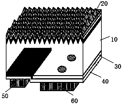
A solar cell and assembly method technology, applied in the direction of electrical components, circuits, photovoltaic power generation, etc., can solve the problems of limited wiring space, low wiring density, and poor flexibility, and achieve less wiring space restrictions and high wiring density. High, cost-reducing effects
- Summary
- Abstract
- Description
- Claims
- Application Information
AI Technical Summary
Problems solved by technology
Method used
Image
Examples
Embodiment 1
[0034] Embodiment 1 Assembly method X1 of solar cell module
[0035] Place the flexible circuit board with a thickness of 0.1mm under the printing machine and fix it well. The design size of the stencil opening of the printing machine corresponds to the electrode position of the IBC cell, and the thickness of the stencil is 0.1mm. The SnBi alloy solder paste is printed on the flexible circuit board with a printing machine, and the hanging pressure is 5kg, and the printing speed is 25mm / sec. Put it into a reflow oven, set the peak temperature of the reflow oven to 190°C, and complete the final soldering.
Embodiment 2
[0036] Embodiment 2 Assembly method X2 of solar cell module
[0037] Place the flexible circuit board with a thickness of 0.25mm under the printing machine and fix it well. The design size of the stencil opening of the printing machine corresponds to the electrode position of the IBC cell, and the thickness of the stencil is 0.08mm. The SnBiCu alloy solder paste is printed on the flexible circuit board with a printing machine, and the hanging pressure is 6kg and the printing speed is 50mm / sec. Put it into a reflow oven, set the peak temperature of the reflow oven to 190°C, and complete the final soldering.
Embodiment 3
[0038] Embodiment 3 Assembly method of solar cell module X3
[0039]Place the flexible circuit board with a thickness of 0.4mm under the printing machine and fix it well. The design size of the stencil opening of the printing machine corresponds to the electrode position of the IBC cell, and the thickness of the stencil is 0.15mm. The SnSbBi alloy solder paste is printed on the flexible circuit board with a printing machine, the hanging pressure is 7kg, and the printing speed is 75mm / sec. Put it into a reflow oven, set the peak temperature of the reflow oven to 190°C, and complete the final soldering.
PUM
| Property | Measurement | Unit |
|---|---|---|
| thickness | aaaaa | aaaaa |
Abstract
Description
Claims
Application Information
 - R&D
- Intellectual Property
- Life Sciences
- Materials
- Tech Scout
- Unparalleled Data Quality
- Higher Quality Content
- 60% Fewer Hallucinations
Browse by: Latest US Patents, China's latest patents, Technical Efficacy Thesaurus, Application Domain, Technology Topic, Popular Technical Reports.
© 2025 PatSnap. All rights reserved.Legal|Privacy policy|Modern Slavery Act Transparency Statement|Sitemap|About US| Contact US: help@patsnap.com


