Fin field effect transistor forming method and semiconductor structure

A technology of fin field effect transistors and fins, which is applied in semiconductor devices, semiconductor/solid-state device manufacturing, transistors, etc., and can solve problems such as complex processes

Active Publication Date: 2020-12-25
SEMICON MFG INT (SHANGHAI) CORP +1
View PDF3 Cites 0 Cited by
  • Summary
  • Abstract
  • Description
  • Claims
  • Application Information

AI Technical Summary

Problems solved by technology

[0005] However, the process of forming fin field effect transistors in the prior art is complicated

Method used


Image

  • Fin field effect transistor forming method and semiconductor structure
  • Fin field effect transistor forming method and semiconductor structure
  • Fin field effect transistor forming method and semiconductor structure

Examples


Embodiment Construction

[0032] It can be seen from the background art that the process of forming the fin field effect transistor in the prior art is complicated.

[0033] With the development of devices toward miniaturization and miniaturization, the forming process of FinFET becomes more and more complicated, especially the process steps of forming the fins in FinFET become more and more cumbersome.

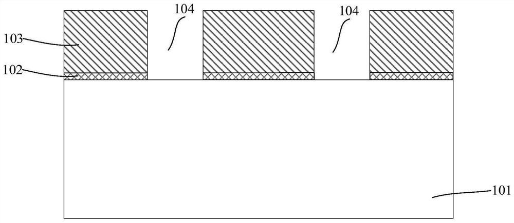
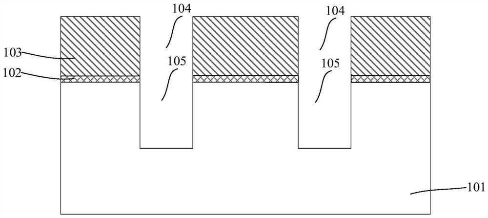
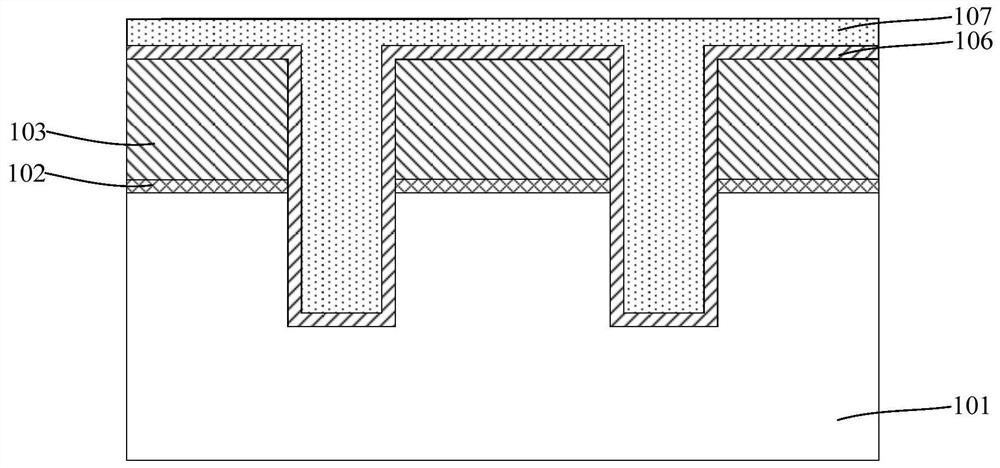
[0034] In order to solve the above problems, the present invention provides a method for forming a fin field effect transistor, comprising: providing a substrate; forming a mask layer on the substrate, the mask layer having a first opening exposing the substrate ; using the mask layer as a mask, etch and remove the base of the first thickness along the first opening, forming a second opening in the base; filling the cores in the first opening and the second opening layer; remove the mask layer to expose part of the core layer sidewalls; form sidewalls on the exposed core layer sidewalls and part of th...


PUM

PropertyMeasurementUnit
thicknessaaaaaaaaaa
thicknessaaaaaaaaaa
thicknessaaaaaaaaaa

Abstract

The invention discloses a fin field effect transistor forming method and a semiconductor structure. The forming method comprises steps: a mask layer is formed on a base, wherein the mask layer is internally provided with a first opening exposing part of the base; with the mask layer as a mask, a base with a first thickness is etched and removed along the first opening, and a second opening is formed in the base; the first opening and the second opening are filled with core layers; the mask layer is removed, and part of core layer side walls is exposed; spacers are formed on the exposed core layer side walls and part of the base, and a third opening is formed between spacers on adjacent core layer side walls; with the spacers as masks, a base with a second thickness is etched and removed along the third opening, and the etched base forms a substrate and separate fins protruding from the substrate; and after the substrate and the fins are formed, the core layers are removed. The fin field effect transistor forming process steps are simplified, and the fin field effect transistor forming method is optimized.

Description

technical field [0001] The invention relates to the technical field of semiconductor manufacturing, in particular to a method for forming a fin field effect transistor and a semiconductor structure. Background technique [0002] With the continuous development of semiconductor process technology, the development trend of semiconductor process nodes following Moore's Law continues to decrease. In order to adapt to the reduction of process nodes, the channel length of MOSFET field effect transistors has to be continuously shortened. The shortening of the channel length has the advantages of increasing the die density of the chip and increasing the switching speed of the MOSFET field effect tube. [0003] However, as the channel length of the device is shortened, the distance between the source and the drain of the device is also shortened, so that the control ability of the gate to the channel becomes worse, resulting in the phenomenon of subthreshold leakage, namely So-call...

Claims


Application Information

Patent Timeline
Patent Type & Authority Patents(China)
IPC IPC(8): H01L21/8234H01L27/088H01L21/336
CPCH01L21/823431H01L27/0886H01L29/66787
Inventor 李勇
Owner SEMICON MFG INT (SHANGHAI) CORP
Why Eureka
Try Eureka