Manufacturing method for controlling independent pore size and independent wire thickness

A production method and technology of independent lines, applied in printed circuit manufacturing, electrical components, printed circuits, etc., can solve the problems of complex production process of circuit boards, uncontrollable control of independent hole diameter and independent line thickness of circuit boards, etc., to achieve convenient upgrading sexual effect

Inactive Publication Date: 2018-05-08
KIN YIP TECHNOLDGY ELECTRONICS HUI ZHOUCO LTD
View PDF6 Cites 2 Cited by
  • Summary
  • Abstract
  • Description
  • Claims
  • Application Information

AI Technical Summary

Problems solved by technology

As the number of layers of circuit boards increases, the number of presses during production also increases, and the production process of circuit boards becomes more and more complicated.
Existing circuit boards cannot control the independent hole diameter and independent line thickness during production. Therefore, it is necessary to design a manufacturing method that controls the independent hole diameter and independent line thickness.

Method used


Image

  • Manufacturing method for controlling independent pore size and independent wire thickness

Examples


Embodiment Construction

[0024] The following will clearly and completely describe the technical solutions in the embodiments of the present invention with reference to the accompanying drawings in the embodiments of the present invention. Obviously, the described embodiments are only some, not all, embodiments of the present invention. Based on the embodiments of the present invention, all other embodiments obtained by persons of ordinary skill in the art without making creative efforts belong to the protection scope of the present invention.

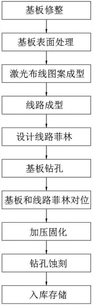
[0025] see figure 1 , the present invention provides a technical solution: a method for controlling the diameter of independent holes and the thickness of independent lines, comprising the following steps:

[0026] 1) Substrate trimming: the substrate is cut into the required size of the circuit board by the substrate cutting machine, and polished by the grinding machine, and it is ready for use after the processing is completed;

[0027] 2) Substrate surface...


PUM


Abstract

The invention discloses a manufacturing method for controlling an independent pore size and an independent wire thickness, which comprises the following steps of substrate dressing, substrate surfacetreatment, laser wiring pattern forming, line forming, line film design, substrate drilling, substrate and line film alignment, pressurized curing, borehole etching and warehousing storage. In the first step, the rotating speed of a grinding machine is 400-550 r / min; in the third step, the laser modulation frequency is 1200-5000 Hz, the pulse width is 60-150 ns and the average laser power is 10-200 W; in the second step, nonmetallic light induced catalyst aldehydes are solid or liquid or gaseous three-component alcohol, and the thermoplastic bearing materials are polyvinyl chloride, polycarbonate and polybutylene terephthalate; and in the sixth step, after the substrate is loaded to a vacuum sucker, an alignment mark is used to enable a drilling beam to be matched with a circuit board. Thestructure is simple, the use is convenient, the pore size and the circuit board thickness can be accurately controlled, and the use convenience is effectively enhanced.

Description

technical field [0001] The invention relates to the technical field of circuit board production, in particular to a manufacturing method for controlling the diameter of independent holes and the thickness of independent lines. Background technique [0002] With the continuous development of electronic communication technology, communication products have more and more functions. In order to better utilize the functions of electronic products, most of the current high-end mobile electronic devices are equipped with touch screens, and the size of the screens is gradually increasing, which results in a double increase in power consumption. In order to increase the standby time of electronic products, manufacturers minimize the size of circuit boards during design to increase the capacity of batteries; 50% or less of the size. The function of the circuit board increases and the volume decreases, resulting in a denser layout of circuit board components and a continuous increase...

Claims


Application Information

Patent Timeline
Patent Type & Authority Applications(China)
IPC IPC(8): H05K3/00H05K3/18
Inventor 石继龙毛敏
Owner KIN YIP TECHNOLDGY ELECTRONICS HUI ZHOUCO LTD
Why Eureka
Try Eureka