
Low cross-axis sensitivity piezoresistive accelerometer structure and manufacturing method thereof

A technology of an accelerometer and a manufacturing method, which are applied in the directions of velocity/acceleration/shock measurement, acceleration measurement, acceleration measurement using inertial force, etc., can solve the problems of high cost, complex process, reduced lateral sensitivity, etc., and achieve small cross-axis sensitivity Effect

Inactive Publication Date: 2018-05-08
CHINA JILIANG UNIV
View PDF3 Cites 8 Cited by
  • Summary
  • Abstract
  • Description
  • Claims
  • Application Information

AI Technical Summary

Problems solved by technology

Electroplating a copper or gold layer on the mass block can move the center of gravity of the mass block to the neutral plane of the beam, and can also reduce the lateral sensitivity, but the process is complicated and the cost is high

Method used


Image

  • Low cross-axis sensitivity piezoresistive accelerometer structure and manufacturing method thereof
  • Low cross-axis sensitivity piezoresistive accelerometer structure and manufacturing method thereof
  • Low cross-axis sensitivity piezoresistive accelerometer structure and manufacturing method thereof

Examples


Embodiment 1

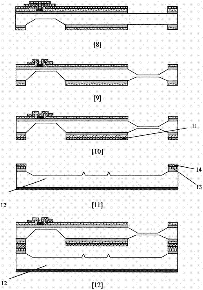
[0034] Embodiment 1: The thickness of the original silicon wafer is 380 microns, the designed thickness of the sensing beam 3 is 5 microns, and the designed thickness of the support beam 2 is 30 microns. The production process determined based on the above data is as follows:

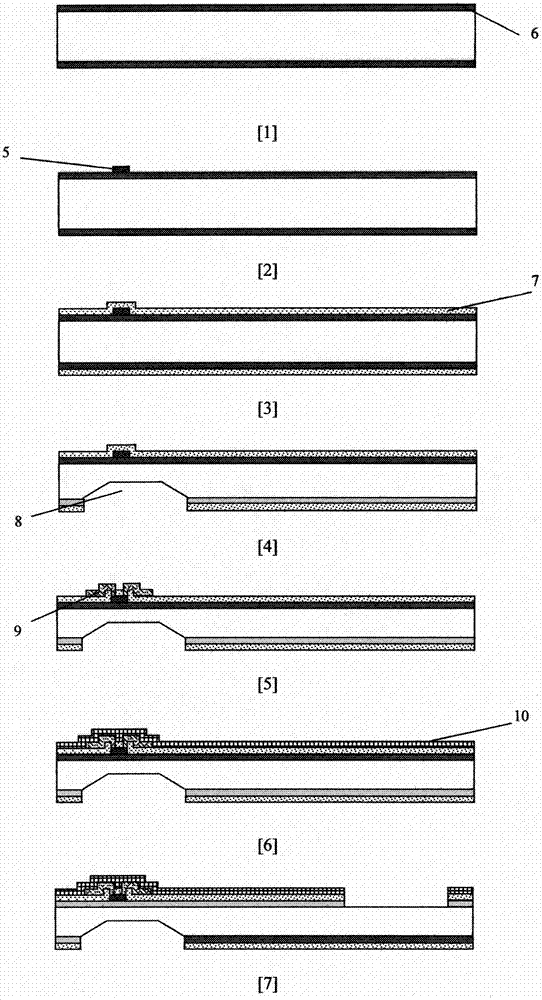
[0035] [1] The original silicon wafer for making the sensor chip is a (100)-sided, double-sided polished silicon wafer with a thickness of 380 microns, and a silicon dioxide film 6 with a thickness of 0.6 microns is produced on the surface of the silicon wafer by thermal oxidation. (see attached figure 2 [1])

[0036] [2] A 0.7-micron polysilicon film was deposited by low-pressure chemical vapor deposition, boron was diffused at high temperature, and the sheet resistance was 300Ω / □, and the varistor 5 was etched by photolithography. (see attached figure 2 [2])

[0037] [3] A 0.25-micron LPCVD silicon nitride film 7 was deposited by low-pressure chemical vapor deposition technology. (see attached ...


PUM


Abstract

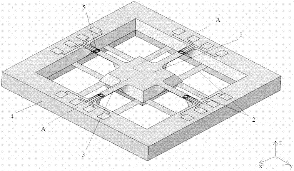
The invention discloses a low cross-axis sensitivity piezoresistive accelerometer structure and a manufacturing method thereof and belongs to the field of micro-electro-mechanical systems. A low cross-axis sensitivity piezoresistive accelerometer is formed by a mass block (1), eight support beams (2), four sensing beams (3) and a frame (4). The center of gravity of the mass block (1) is located ina neutral plane of the support beams (2). The upper surfaces of the sensing beams (3) are located on the surface of a chip such that piezoresistors (5) are made on the surfaces of the sensing beams.The thickness of the sensing beams is far smaller than that of the support beams. Under the action of Z-axis acceleration on the surface of a vertical chip, the mass block (1) moves in a Z-axis direction and drives the sensing beams (3) to move together, the strain of the sensing beams (3) is detected by the piezoresistors (5), thus Z-axis acceleration is obtained. Since the center of gravity of the mass block (1) is located in the neutral plane of the support beams (2), the deflection angle of the mass block (1) under X-axis or Y-axis acceleration within the chip surface is small, and so thestructure has small cross-axis sensitivity.

Description

technical field [0001] The invention relates to a piezoresistive accelerometer structure and manufacturing method with low cross-axis sensitivity, in particular to a piezoresistive accelerometer structure and manufacturing method with low cross-axis sensitivity manufactured by mask-less mask etching technology, belonging to micro Electro-mechanical systems (Micro-Electro-Mechanical Systems, MEMS) field. Background technique [0002] Micro accelerometer is an important type of mechanical quantity sensor, with the advantages of small size, light weight, low power consumption and cost, easy integration, and mass production. It is not only the core component of micro inertial measurement combination, but also widely used in vehicle control. , high-speed railway, robot, industrial automation, prospecting, toys, medical treatment and other fields. Micro accelerometers can be divided into linear accelerometers and pendulum accelerometers according to the movement mode of the detec...

Claims


Application Information

Patent Timeline
Patent Type & Authority Applications(China)
IPC IPC(8): G01P15/12G01P15/08
CPCG01P15/08G01P15/12G01P2015/0871
Inventor 韩建强牛文举赵正前
Owner CHINA JILIANG UNIV
Learn More