
Metal cavity-based surface plasmon laser

A technology of surface plasmons and lasers, applied in lasers, laser components, semiconductor lasers, etc., can solve the problems of large reflection loss, difficult to control the physical size and shape of nanowires precisely, and achieve low loss and strong binding ability , The effect of reducing reflection loss

Active Publication Date: 2018-04-24
HUAQIAO UNIVERSITY
View PDF8 Cites 13 Cited by
  • Summary
  • Abstract
  • Description
  • Claims
  • Application Information

AI Technical Summary

Problems solved by technology

However, since the reflectance of surface plasmon waves on the nanowire end face is <20%, the reflection loss of this resonator is very large, making this semiconductor nanowire-based laser work only in an ultra-low temperature environment.
Furthermore, since the nanowires are grown by methods such as chemical vapor deposition, the physical size and shape of the nanowires (i.e., the resonant cavity of the laser) are difficult to precisely control

Method used


Image

  • Metal cavity-based surface plasmon laser
  • Metal cavity-based surface plasmon laser
  • Metal cavity-based surface plasmon laser

Examples


Embodiment Construction

[0024] The present invention will be further elaborated below in conjunction with the accompanying drawings and specific embodiments.

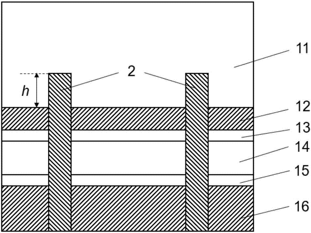
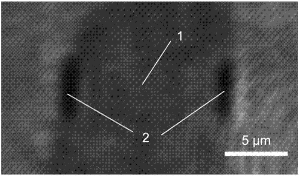
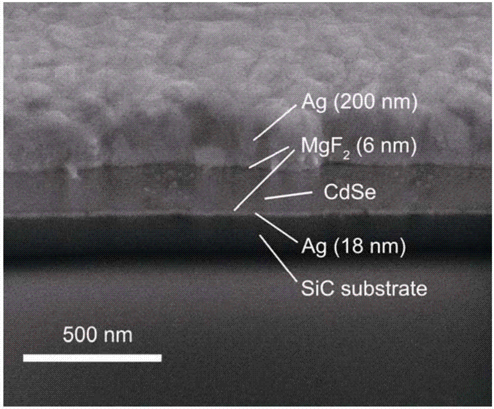
[0025] Such as figure 1 and figure 2 As shown, the metal cavity-based surface plasmon laser of this embodiment includes: a surface plasmon waveguide 1 and a metal cavity 2; wherein the surface plasmon waveguide 1 further includes a high refractive index transparent substrate layer 11, Metal thin film layer 12, insulating medium layer 13, gain medium layer 14, insulating medium layer 15 and metal thick film layer 16; Metal thin film layer 12 is plated on the transparent substrate layer 11, insulating medium layer 13 is plated on the metal thin film layer 12, The gain medium layer 14 is a semiconductor nanobelt, which is closely attached to the surface of the insulating medium layer 13 without gaps. The insulating medium layer 15 is plated on the gain medium layer 14 , and the metal thick film layer 16 is plated on the insulating medium layer ...


PUM

PropertyMeasurementUnit
Thicknessaaaaaaaaaa

Abstract

The invention discloses a metal cavity-based surface plasmon laser. The metal cavity-based surface plasmon laser comprises a surface plasmon waveguide and a metal cavity. The metal cavity is embeddedinto the surface plasmon waveguide by an etching technology and serves as a resonant cavity of a laser, so that the shape and the size of the metal cavity can be precisely controlled. The reflectivityof a cavity mirror of the metal cavity to a surface plasmon mode in the cavity is higher than 90%, so that the Q value of the surface plasmon laser in the metal cavity is as high as 1170. The surfaceplasmon laser uses the metal cavity as the resonant cavity for the laser, and has the advantages of a small physical size, a large quality factor, capability of precisely controlling the shape and the size, a simple and mature preparation technology, room-temperature working, compatibility with an electronic chip and the like.

Description

technical field [0001] The invention relates to a micro laser, in particular to a surface plasmon laser based on a metal cavity. Background technique [0002] For half a century, lasers are developing rapidly towards smaller volume, faster modulation speed, higher power, and higher efficiency. However, traditional semiconductor lasers are limited by the diffraction limit, and cannot exceed the half-wavelength of the optical field in terms of both the optical field mode size and the device physical size. Therefore, how to further reduce the size of lasers, provide coherent light sources for future nanoscale integrated optical chips, and realize ultra-small lasers at the nanoscale have always been key issues to be solved in the field of laser technology. [0003] Recent studies have shown that surface plasmons localized at the metal-dielectric interface can confine the optical field to subwavelength or even deep subwavelength scales, thus breaking the diffraction limit. Surf...

Claims


Application Information

Patent Timeline
IPC IPC(8): H01S5/028H01S5/04H01S5/10H01S5/30
CPCH01S5/028H01S5/041H01S5/10H01S5/30
Inventor 温秋玲张家森徐西鹏
Owner HUAQIAO UNIVERSITY
Learn More