Ohmic-contact and Schottky contact super-barrier rectifier and manufacturing method therefor
A super-barrier rectification and Schottky contact technology, which is applied in semiconductor/solid-state device manufacturing, semiconductor devices, electrical components, etc., can solve the problems of large forward voltage drop, weak overcurrent capability of rectifiers, etc., and can withstand overcurrent Improved capability, increased ohmic contact design, reduced effect of forward voltage
- Summary
- Abstract
- Description
- Claims
- Application Information
AI Technical Summary
Problems solved by technology
Method used
Image
Examples
Embodiment 1
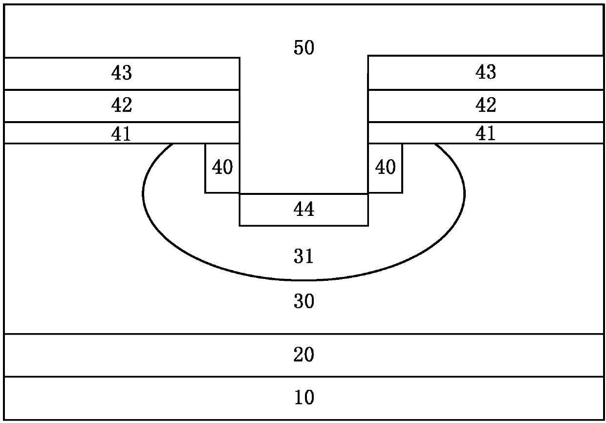
[0045] Such as figure 1 As shown, a super barrier rectifier with ohmic contact and Schottky contact is characterized in that it includes a lower electrode layer 10, a heavily doped first conductivity type substrate layer 20, a lightly doped first conductivity type epitaxial layer 30, a second Two-conductivity type body region 31 , Schottky contact region 40 , gate dielectric layer 41 , gate electrode layer 42 , masking dielectric layer 43 , ohmic contact region 44 and upper electrode layer 50 .
[0046] The heavily doped substrate layer 20 of the first conductivity type covers the lower electrode layer 10 .
[0047] The lightly doped first conductive type epitaxial layer 30 covers the heavily doped first conductive type substrate layer 20 .
[0048] The body region 31 of the second conductivity type covers part of the surface of the epitaxial layer 30 of the lightly doped first conductivity type.
[0049] The ohmic contact region 44 covers part of the surface above the secon...
Embodiment 2
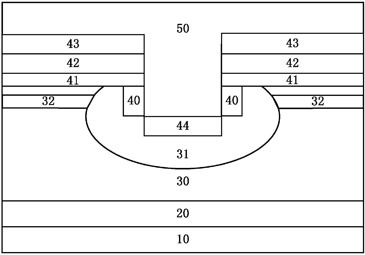
[0059] Such as figure 2 As shown, a super barrier rectifier with ohmic contact and Schottky contact is characterized in that it includes a lower electrode layer 10, a heavily doped first conductivity type substrate layer 20, a lightly doped first conductivity type epitaxial layer 30, a second Two conductivity type body region 31 , first conductivity type enhancement layer 32 , Schottky contact region 40 , gate dielectric layer 41 , gate electrode layer 42 , masking dielectric layer 43 , ohmic contact region 44 and upper electrode layer 50 .
[0060]The heavily doped first conductivity type substrate layer 20 covers the lower electrode layer 10;
[0061] The lightly doped first conductivity type epitaxial layer 30 covers the heavily doped first conductivity type substrate layer 20;
[0062] The second conductivity type body region 31 covers part of the surface above the lightly doped first conductivity type epitaxial layer 30;
[0063] The enhancement layer 32 of the first c...
Embodiment 3
[0074] A super barrier rectifier with ohmic contact and Schottky contact, characterized in that it includes a lower electrode layer 10, a heavily doped first conductivity type substrate layer 20, a lightly doped first conductivity type epitaxial layer 30, a second conductivity type Body region 31 , Schottky contact region 40 , gate dielectric layer 41 , gate electrode layer 42 , masking dielectric layer 43 , ohmic contact region 44 and upper electrode layer 50 .
[0075] A method for manufacturing an ohmic contact and a Schottky contact super barrier rectifier is characterized in that it comprises the following main steps:
[0076] Select the first conductivity type as N type, and the second conductivity type as P type;
[0077] 1) Covering the N-type epitaxial layer 30 on the N+ type substrate layer 20; the N+ type substrate layer 20 is an arsenic substrate with a doping concentration above the 19th power; the N-type epitaxial layer 30 is an arsenic substrate with an impurity...
PUM
| Property | Measurement | Unit |
|---|---|---|
| thickness | aaaaa | aaaaa |
Abstract
Description
Claims
Application Information
 - R&D Engineer
- R&D Manager
- IP Professional
- Industry Leading Data Capabilities
- Powerful AI technology
- Patent DNA Extraction
Browse by: Latest US Patents, China's latest patents, Technical Efficacy Thesaurus, Application Domain, Technology Topic, Popular Technical Reports.
© 2024 PatSnap. All rights reserved.Legal|Privacy policy|Modern Slavery Act Transparency Statement|Sitemap|About US| Contact US: help@patsnap.com


