ga 2 o 3 Fabrication method of thin film transistor
A thin film transistor, ga2o3 technology, applied in transistors, semiconductor/solid-state device manufacturing, semiconductor devices and other directions, can solve the problems of low utilization rate of raw materials, high reaction temperature, environmental pollution, etc., to achieve easy control of the experimental process, good uniformity, The effect of easy response
- Summary
- Abstract
- Description
- Claims
- Application Information
AI Technical Summary
Problems solved by technology
Method used
Image

Examples
Embodiment 1
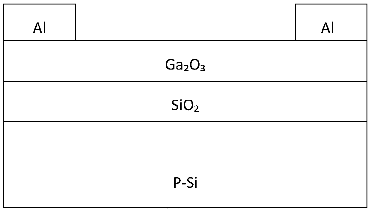
[0045] Embodiment 1, making a layer of film Ga with a thickness of 8nm 2 o 3 thin film transistor.
[0046] Step 1, preparing an aqueous precursor solution.
[0047] Take Ga(NO 3 ) 3 Solid powder 0.26g, deionized water 10mL, Ga(NO 3 ) 3 The solid powder was dissolved in deionized water to make a concentration of 0.1mol / L Ga(NO 3 ) 3 Precursor aqueous solution.
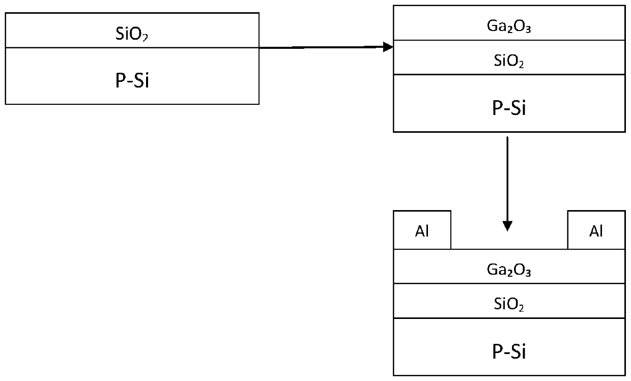
[0048] Step 2, cleaning the silicon wafer.
[0049] Select a silicon wafer containing a 200nm thick silicon oxide insulating layer as the substrate, and clean it as follows:
[0050] Ultrasonic soaking in acetone solution for 10 minutes, then ultrasonic soaking in ethanol solution for 10 minutes, and finally ultrasonic soaking in deionized water for 10 minutes to complete the cleaning of the silicon wafer substrate.
[0051] Step 3, decontamination of the silicon oxide surface.
[0052] Use the oxygen plasma of the glue remover to decontaminate the surface of the cleaned silicon wafer, that is, place the cle...
Embodiment 2
[0059] Embodiment 2, making a layer of film Ga with a thickness of 5nm 2 o 3 thin film transistor.
[0060] Step 1, preparing an aqueous precursor solution.
[0061] Take Ga(NO 3 ) 3 Solid powder 0.768g, deionized water 10mL, Ga(NO 3 ) 3 The solid powder was dissolved in deionized water to make a concentration of 0.03mol / L Ga(NO 3 ) 3 Precursor aqueous solution.
[0062] Step two, cleaning the silicon wafer.
[0063] The specific implementation of this step is the same as step 2 of embodiment 1.
[0064] Step 3, decontamination of the silicon oxide surface.
[0065] The specific implementation of this step is the same as step 3 of embodiment 1.
[0066] Step 4, spin coating the aqueous solution of the precursor.
[0067] Drop the precursor aqueous solution on the silicon oxide layer of the decontaminated silicon wafer with a dropper, and spin coat it for 30 seconds at a speed of 4000rpm using a homogenizer to form a uniform layer of Ga(NO 3 ) 3 film.
[0068] St...
Embodiment 3
[0072] Embodiment 3, making a layer of film Ga with a thickness of 15nm 2 o 3 thin film transistor.
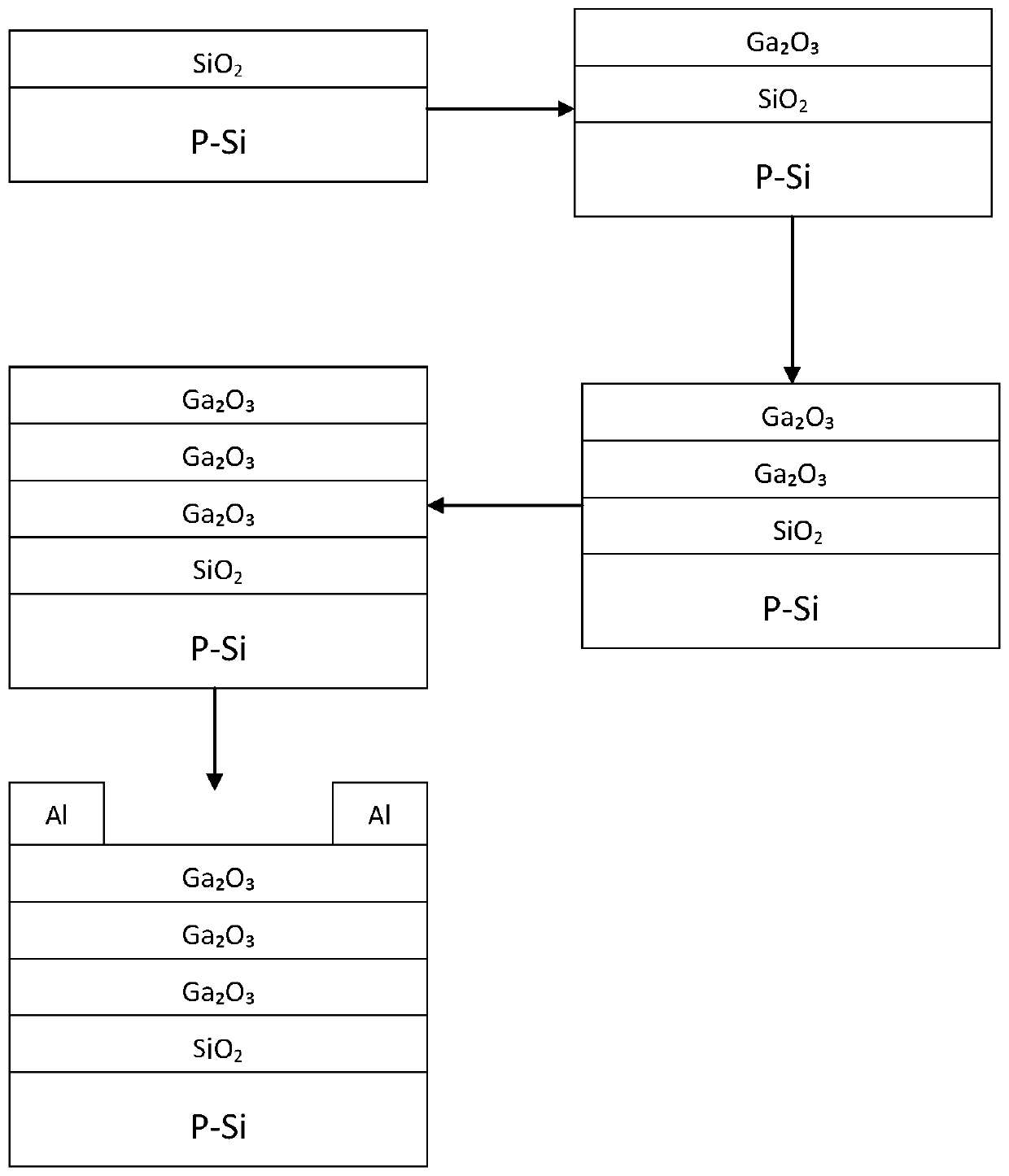
[0073] Step A, preparing an aqueous precursor solution.
[0074] Take Ga(NO 3 ) 3 Solid powder 1.28g, deionized water 10mL, Ga(NO 3 ) 3 The solid powder was dissolved in deionized water to make a concentration of 0.5mol / L Ga(NO 3 ) 3 Precursor aqueous solution.
[0075] Step B, cleaning the silicon wafer.
[0076] The specific implementation of this step is the same as step 2 of embodiment 1.
[0077] Step C, decontamination of the silicon oxide surface.
[0078] The specific implementation of this step is the same as step 3 of embodiment 1.
[0079] Step D, spin coating the aqueous solution of the precursor.
[0080] Drop the precursor aqueous solution on the silicon oxide layer of the decontaminated silicon wafer with a dropper, and spin coat it for 30 seconds at a speed of 2000rpm using a homogenizer to form a uniform layer of Ga(NO 3 ) 3 film.
[0081] Step ...
PUM
| Property | Measurement | Unit |
|---|---|---|
| thickness | aaaaa | aaaaa |
| thickness | aaaaa | aaaaa |
| thickness | aaaaa | aaaaa |
Abstract
Description
Claims
Application Information
 - R&D
- Intellectual Property
- Life Sciences
- Materials
- Tech Scout
- Unparalleled Data Quality
- Higher Quality Content
- 60% Fewer Hallucinations
Browse by: Latest US Patents, China's latest patents, Technical Efficacy Thesaurus, Application Domain, Technology Topic, Popular Technical Reports.
© 2025 PatSnap. All rights reserved.Legal|Privacy policy|Modern Slavery Act Transparency Statement|Sitemap|About US| Contact US: help@patsnap.com