Metal mask for vapor deposition, method for producing metal mask for vapor deposition, and substrate for forming metal mask for vapor deposition
A metal mask and mask technology, applied in metal material coating process, vacuum evaporation plating, semiconductor/solid-state device manufacturing, etc., can solve the problem of inability to cope with the high density of mask holes
- Summary
- Abstract
- Description
- Claims
- Application Information
AI Technical Summary
Problems solved by technology
Method used
Image
Examples
Embodiment 1
[0081] [Preparation of resist layer composition]
[0082] In paragraph 0053, 70 parts by weight of pentaerythritol triacrylate, 123 parts by weight of Cardo resin (V259ME: manufactured by Nippon Steel & Sumikin Chemical Co., Ltd.), and 14 parts by weight of a photopolymerization initiator (IRGACURE907: manufactured by BASF Japan Corporation) (IRGACURE is a registered trademark) was diluted with cyclohexanone so that the solid content of the resist layer composition became 50% by weight to prepare a resist layer composition.
[0083] [Manufacturing of metal masks for vapor deposition]
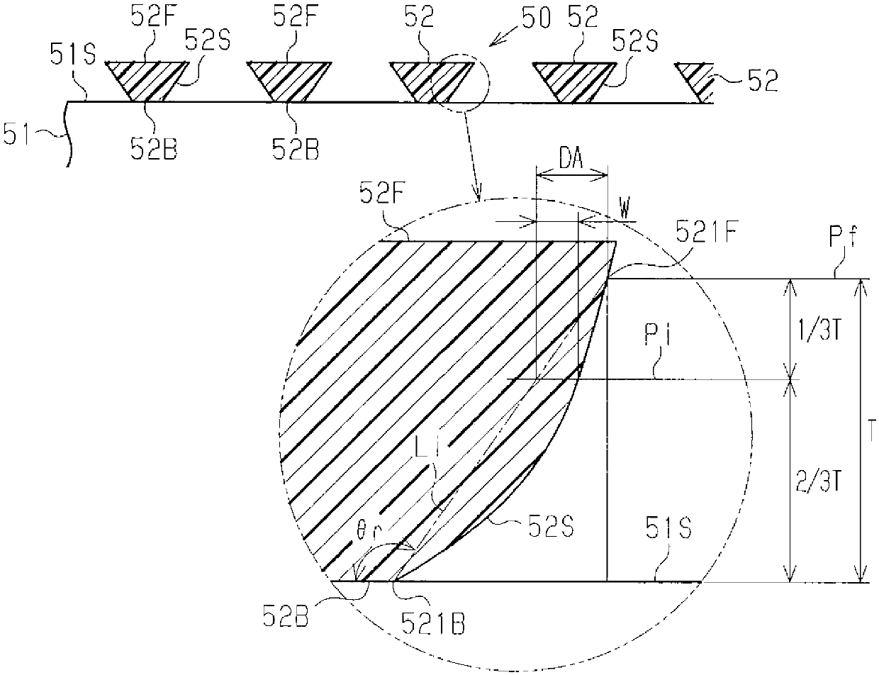
[0084] On the electrode surface 51S of the electrode member 51 , a negative resist layer composition was applied so that the film thickness after drying would be 30 μm. Thereafter, the resist layer composition was dried at 90° C. / 3 minutes using a hot plate, and a high-pressure mercury lamp (intensity of light: illuminance of 365 nm bright line was 40 mW / cm 2 ), exposed to 200mJ / cm through a p...
Embodiment 2
[0087] The mask member of Example 2 was obtained like Example 1 except having changed the developing time in Example 1 to 45 seconds. As a result of observing the cross-sectional shape of the resist pattern with a scanning electron microscope, it was confirmed that the width of the top surface 52B was 35.9 μm, the width of the bottom surface 52F was 62.7 μm, and the resist pattern was in the shape of an inverted truncated cone. In addition, when the cross-sectional shape of the mask member 32 was observed, the inclination angle θ was 73.6°, and [(3×tan θ)×A] / H was 0.16.
Embodiment 3
[0089] Change the exposure amount in Example 1 to 150mJ / cm 2 , and the mask member of Example 3 was obtained in the same manner as in Example 1 except that the development time was changed to 45 seconds. As a result of observing the cross-sectional shape of the resist pattern with a scanning electron microscope, it was confirmed that the width of the top surface 52B was 20.5 μm, the width of the bottom surface 52F was 61.8 μm, and the resist pattern was in the shape of an inverted truncated cone. In addition, when the cross-sectional shape of the mask member 32 was observed, the inclination angle θ was 67.9°, and [(3×tan θ)×A] / H was 0.29.
PUM
| Property | Measurement | Unit |
|---|---|---|
| thickness | aaaaa | aaaaa |
| thickness | aaaaa | aaaaa |
| width | aaaaa | aaaaa |
Abstract
Description
Claims
Application Information
 - R&D
- Intellectual Property
- Life Sciences
- Materials
- Tech Scout
- Unparalleled Data Quality
- Higher Quality Content
- 60% Fewer Hallucinations
Browse by: Latest US Patents, China's latest patents, Technical Efficacy Thesaurus, Application Domain, Technology Topic, Popular Technical Reports.
© 2025 PatSnap. All rights reserved.Legal|Privacy policy|Modern Slavery Act Transparency Statement|Sitemap|About US| Contact US: help@patsnap.com


