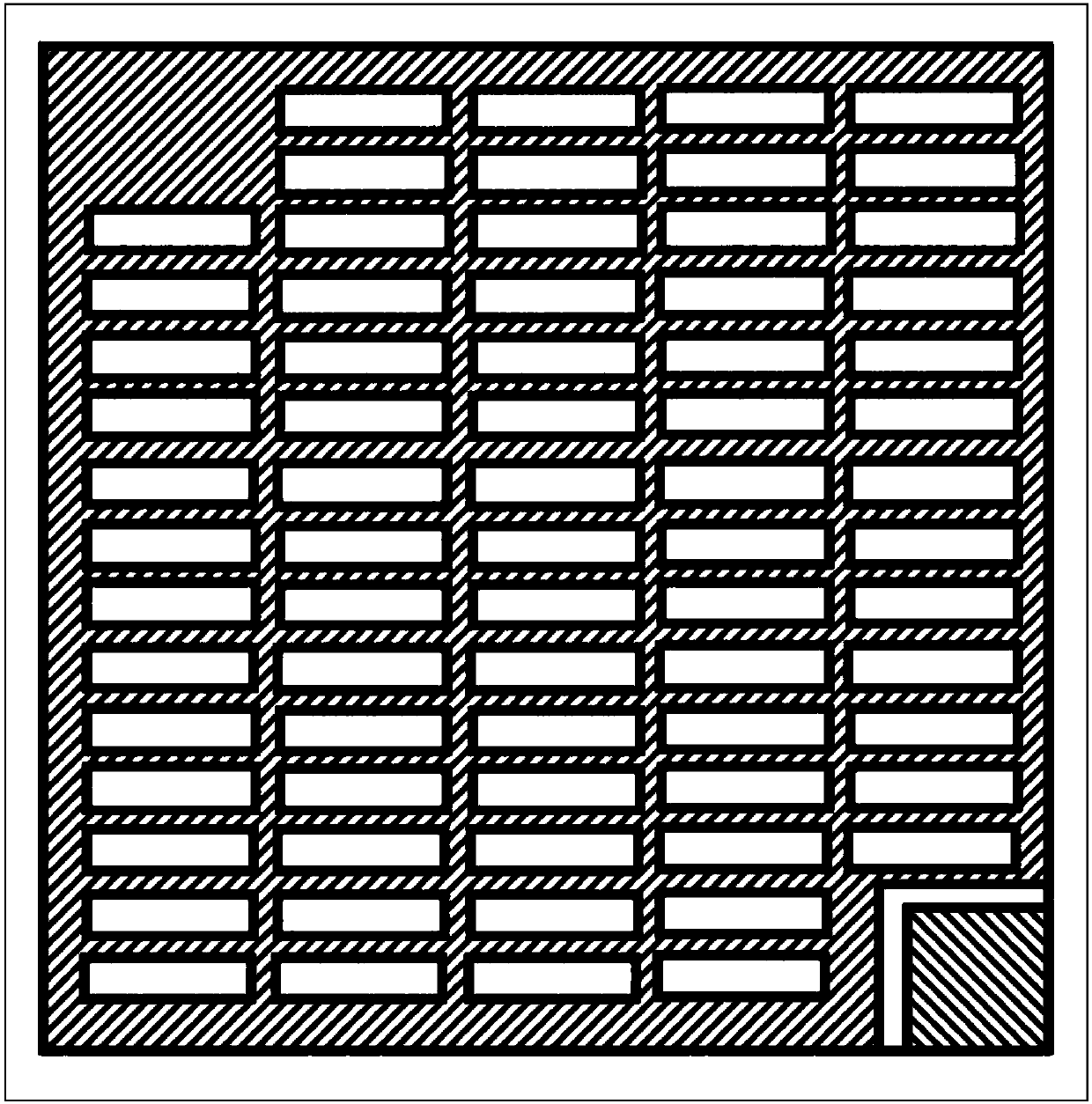
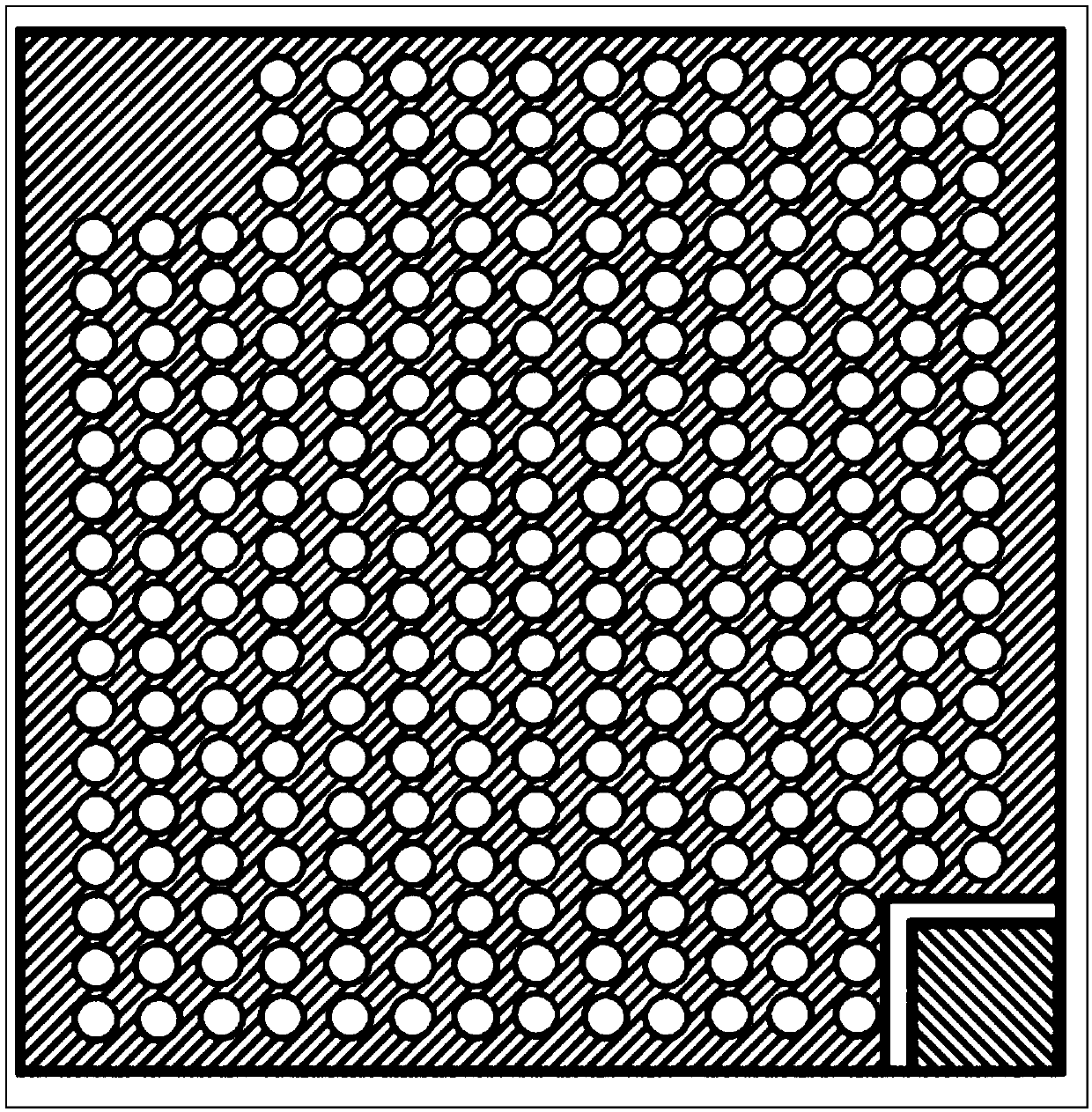
Vertical structure LED chip based on photonic crystal and preparation method of vertical structure LED chip
A technology of LED chips and photonic crystals, applied in nano optics, semiconductor devices, electrical components, etc., can solve the problems of reducing light extraction efficiency, large resistance, etc., achieve excellent photoelectric performance, low production cost, and improve internal thermal field and current distribution The effect of uniformity
- Summary
- Abstract
- Description
- Claims
- Application Information
AI Technical Summary
Problems solved by technology
Method used
Image


Examples
preparation example Construction
[0041] A method for preparing a photonic crystal-based vertical structure LED chip, comprising the following steps:
[0042] A. Put the Si or Cu substrate layer 11 into deionized water and ultrasonically clean it at room temperature for 3-5 minutes to remove the dirt particles on the surface of the Si or Cu substrate layer 11, and then wash with hydrochloric acid, acetone, and ethanol in sequence to remove the surface organic matter. Dry high-purity N 2 Blow dry, pay attention not to use high-purity N 2 plasma;
[0043] B. Put the cleaned and dried Si or Cu substrate layer 11 into a vacuum chamber, and anneal at a high temperature of 700-1200°C for 30-120 minutes to remove the residual carbides on the surface of the Si or Cu substrate layer 11, so as to obtain a clean and flat surface ;
[0044] C. Preparation of Al single crystal metal thin film layer 12: heating Si or Cu substrate layer 11 to 700-1000°C, and filling with 0.5-2 sccm of high-purity N under high vacuum condi...
Embodiment 1
[0058] A method for preparing a photonic crystal-based vertical structure LED chip, comprising the following steps:
[0059] A. Put the Si or Cu substrate layer 11 into deionized water and ultrasonically clean it at room temperature for 3-5 minutes to remove the dirt particles on the surface of the Si or Cu substrate layer 11, and then wash with hydrochloric acid, acetone, and ethanol in sequence to remove the surface organic matter. Dry high-purity N 2 blow dry;
[0060] B. Put the cleaned and dried Si or Cu substrate layer 11 into a vacuum chamber, and anneal at a high temperature of 700-1200°C for 30-120 minutes to remove the residual carbides on the surface of the Si or Cu substrate layer 11, so as to obtain a clean and flat surface ;
[0061] C. Preparation of Al single crystal metal thin film layer 12: heating Si or Cu substrate layer 11 to 850°C, and filling with 1 sccm of high-purity N under high vacuum conditions 2 , heating the Al source to 1100°C to volatilize th...
Embodiment 2
[0072] A method for preparing a photonic crystal-based vertical structure LED chip, comprising the following steps:
[0073] A. Put the Si or Cu substrate layer 11 into deionized water and ultrasonically clean it at room temperature for 3-5 minutes to remove the dirt particles on the surface of the Si or Cu substrate layer 11, and then wash with hydrochloric acid, acetone, and ethanol in sequence to remove the surface organic matter. Dry high-purity N 2 blow dry;
[0074] B. Put the cleaned and dried Si or Cu substrate layer 11 into a vacuum chamber, and anneal at a high temperature of 1200° C. for 60 minutes to remove residual carbides on the surface of the Si or Cu substrate layer 11, thereby obtaining a clean and flat surface;
[0075] C. Preparation of Al single crystal metal thin film layer 12: heating Si or Cu substrate layer 11 to 850°C, and filling with 1 sccm of high-purity N under high vacuum conditions 2 , heating the Al source to 1100°C to volatilize the aluminum...
PUM
| Property | Measurement | Unit |
|---|---|---|
| thickness | aaaaa | aaaaa |
| thickness | aaaaa | aaaaa |
| thickness | aaaaa | aaaaa |
Abstract
Description
Claims
Application Information
 - R&D
- Intellectual Property
- Life Sciences
- Materials
- Tech Scout
- Unparalleled Data Quality
- Higher Quality Content
- 60% Fewer Hallucinations
Browse by: Latest US Patents, China's latest patents, Technical Efficacy Thesaurus, Application Domain, Technology Topic, Popular Technical Reports.
© 2025 PatSnap. All rights reserved.Legal|Privacy policy|Modern Slavery Act Transparency Statement|Sitemap|About US| Contact US: help@patsnap.com