Array substrate, display panel and electronic equipment

A technology for array substrates and display panels, which is applied to circuits, electrical components, and electric solid devices, and can solve problems affecting display effects, large impedance, and data signal distortion, and achieve improved use stability, small impedance, and elimination of data signals distortion effect

Active Publication Date: 2020-11-24
SHANGHAI TIANMA MICRO ELECTRONICS CO LTD
View PDF5 Cites 0 Cited by
  • Summary
  • Abstract
  • Description
  • Claims
  • Application Information

AI Technical Summary

Problems solved by technology

[0003] In the prior art, in order to realize a narrow frame, a commonly used wiring method of the array substrate is the T-wire method. For example, the data lines extending along the first direction and arranged along the second direction can be connected to the The driving chip is electrically connected, and the scanning lines extending along the second direction and arranged along the first direction are directly electrically connected to the driving chip. Since the data signal is transmitted from the driving chip to a specific pixel unit, it needs to pass through the data connection line and the data line, and the impedance is relatively high. Large, resulting in a certain degree of distortion in the data signal, which affects the display effect

Method used


Image

  • Array substrate, display panel and electronic equipment
  • Array substrate, display panel and electronic equipment
  • Array substrate, display panel and electronic equipment

Examples


Embodiment Construction

[0028] The present invention will be further described in detail below in conjunction with the accompanying drawings and embodiments. It should be understood that the specific embodiments described here are only used to explain the present invention, but not to limit the present invention. In addition, it should be noted that, for the convenience of description, only some structures related to the present invention are shown in the drawings but not all structures.

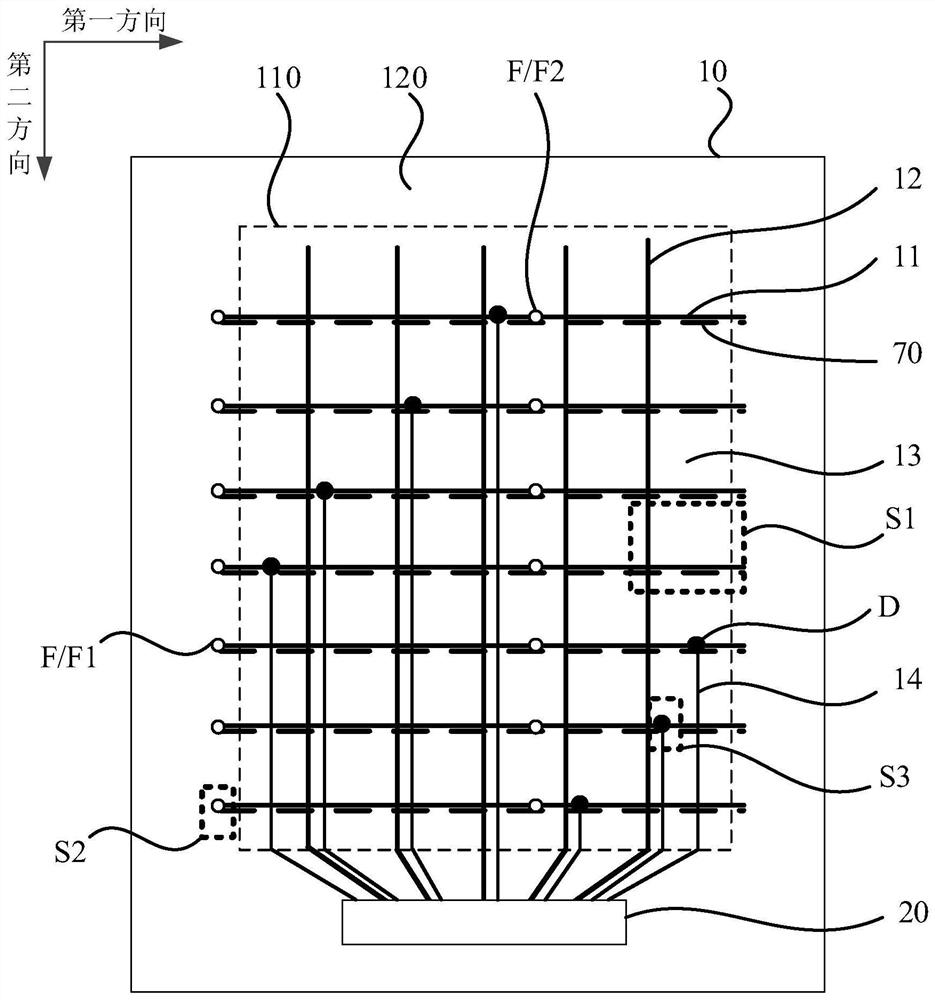
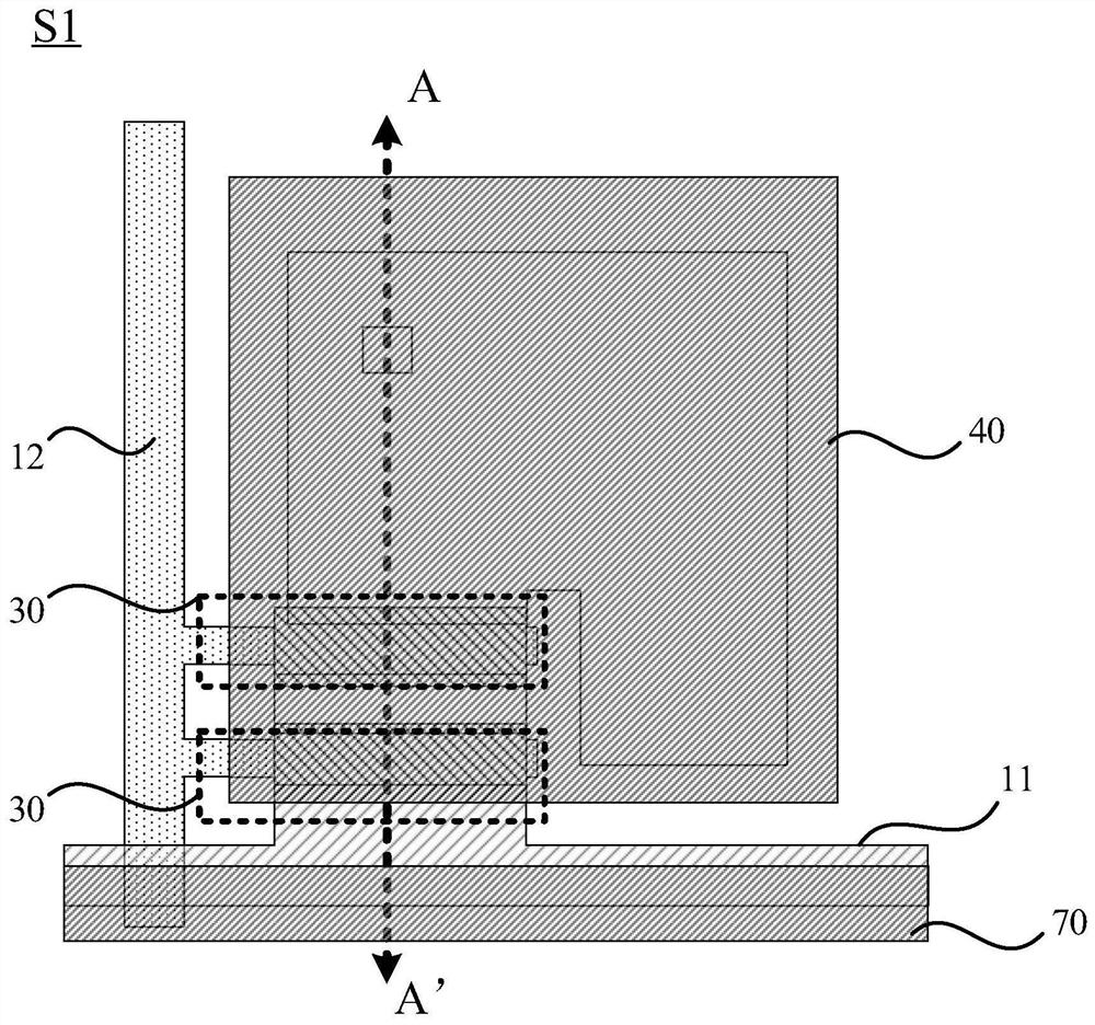
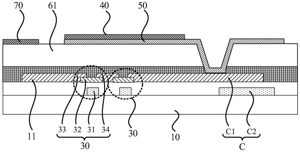
[0029] figure 1 It is a schematic top view structure diagram of an array substrate provided by an embodiment of the present invention, figure 2 for figure 1 A schematic diagram of an enlarged structure of the S1 region in the middle, image 3 for along figure 2 A schematic diagram of a cross-sectional structure in the direction of AA', Figure 4 for figure 1 A schematic diagram of a cross-sectional structure of the S2 region in the middle, combined with figure 1 , figure 2 , image 3 with Figure 4 As ...


PUM


Abstract

The invention provides an array substrate, a display panel and electronic equipment. The array substrate comprises a substrate, thin-film transistors, shading metal layers, a plurality of auxiliary lines, a plurality of data connection lines and a drive chip, wherein each shading metal layer is located at one side, far away from the substrate, of the corresponding thin-film transistor; each auxiliary line is located at one side, far away from the substrate, of a corresponding data line; the auxiliary lines correspond to the data lines one by one; each auxiliary line is separated from the corresponding data line through a first insulating layer and at least two auxiliary line through holes exist, so that each auxiliary line is electrically connected with the corresponding data line; the extension directions of the data connection lines are consistent with those of scanning lines; a first end of each data connection line is electrically connected with the corresponding data line througha data connection line through hole and a second end of each data connection line is electrically connected with the drive chip; and the auxiliary lines and the shading metal layers are arranged on the same layer. According to the array substrate, data signal distortion is reduced or even eliminated, and the display effects of the display panel and the electronic equipment are improved.

Description

technical field [0001] The present invention relates to the field of display technology, in particular to an array substrate, a display panel and electronic equipment. Background technique [0002] For thin-film transistor display technology, the scan line is generally used to control the opening of the thin-film transistor, and the data signal transmitted on the data line is transmitted to the pixel electrode of the pixel unit through the thin-film transistor, and an electric field is generated between the pixel electrode and the common electrode to drive the display function layer. show. Wherein, the display function layer may include organic luminescent material, liquid crystal material or electrophoretic material and the like. [0003] In the prior art, in order to realize a narrow frame, a commonly used wiring method of the array substrate is the T-wire method. For example, the data lines extending along the first direction and arranged along the second direction can b...

Claims


Application Information

Patent Timeline
Patent Type & Authority Patents(China)
IPC IPC(8): H01L27/12
CPCH01L27/1214H01L27/124
Inventor 周一安杜雷许文钦
Owner SHANGHAI TIANMA MICRO ELECTRONICS CO LTD
Why Eureka
Try Eureka