A burr-free photolithography method

A burr-free, lithography technology, used in microlithography exposure equipment, optics, opto-mechanical equipment, etc., can solve the problems of metal layer metal burrs, affecting product yield, difficult to adjust, etc., to improve device electrical properties, improve The effect of device yield and development uniformity

Active Publication Date: 2020-04-21
CHENGDU HIWAFER SEMICON CO LTD
View PDF2 Cites 0 Cited by
  • Summary
  • Abstract
  • Description
  • Claims
  • Application Information

AI Technical Summary

Problems solved by technology

like Figure 1-2 As shown, the slope of the inverted trapezoidal angle is relatively large, and it is difficult to adjust. After metal evaporation, the metal formed on the side wall of the photoresist 2 is easy to adhere to the metal in the filling area 3. When the glue is removed, the photoresist 2, the metal on the sidewall will be carried up together, causing a part of the metal in the filling area 3 that is adhered to the photoresist 2 sidewall metal to be taken away together, so that metal burrs appear in the remaining filling area 3 metal layer 4 5. It affects both the appearance and the product yield

Method used


Image

  • A burr-free photolithography method
  • A burr-free photolithography method
  • A burr-free photolithography method

Examples


Embodiment Construction

[0018] In order to make the purpose, technical solution and advantages of the present application clearer, the present application will be further described in detail below in conjunction with the accompanying drawings and specific embodiments. For simplicity, some technical features known to those skilled in the art are omitted from the following description.

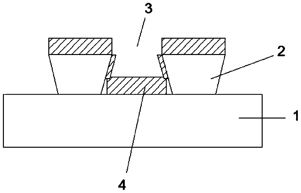
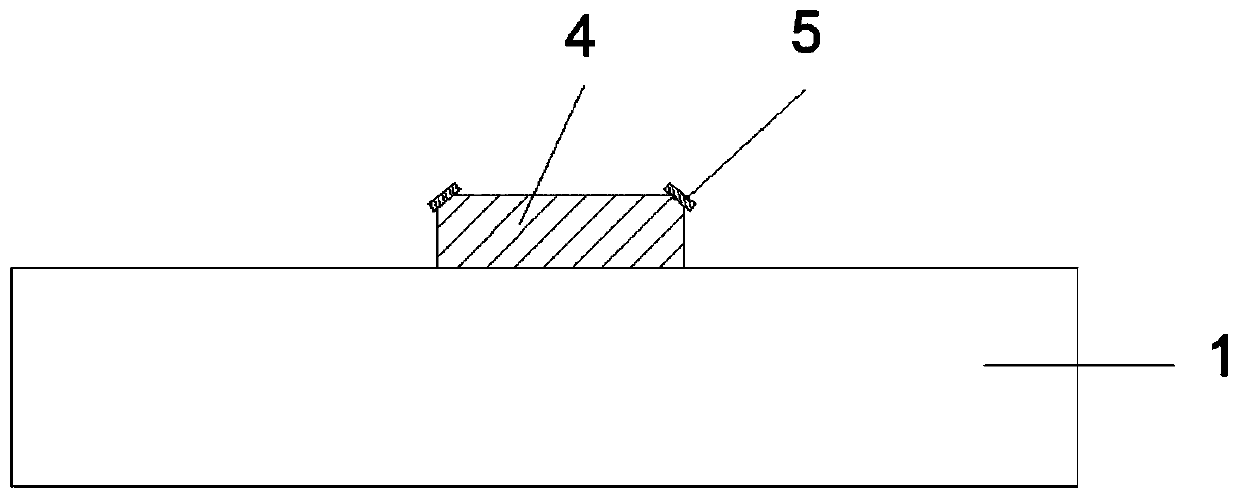
[0019] Such as image 3 As shown, the present embodiment provides a burr-free photolithography method, comprising the following steps:

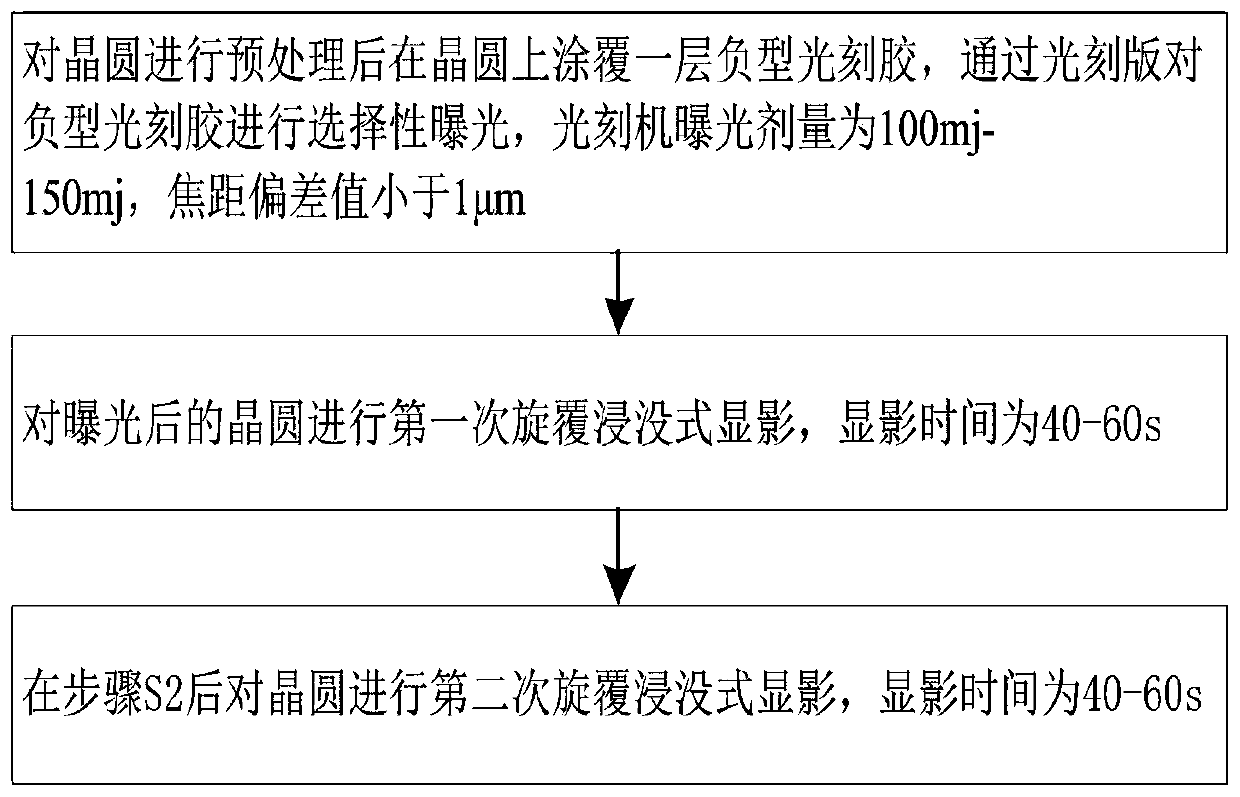
[0020] S11. Perform pretreatment on the wafer 11. Clean the surface of the wafer 11 with deionized water. After cleaning, use a hot plate to remove moisture from the surface of the wafer 11 under the protection of nitrogen. The temperature of the hot plate is 150-250° C., and the baking time is 1~2min;

[0021] S12. Spin-coat a layer of negative photoresist on the wafer 11. The thickness of the negative photoresist must match the thickness of the metal to be evaporated. Generally, t...


PUM


Abstract

The invention relates to the technical field of semiconductor manufacturing and in particular relates to a burr-free photoetching method. The burr-free photoetching method comprises the following steps: S1, after pre-treating a wafer, coating the wafer with one layer of negative photoresist; carrying out selective exposure on the negative photoresist through a photoetching mask, wherein the exposure dosage of a photoetching machine is 100mj to 150mj and the focal distance deviation value is less than 1mu m; S2, carrying out first time of rotary covering and immersing type development on the exposed wafer, wherein the development time is 40s to 60s; S3, carrying out second time of rotary covering and immersing type development on the wafer after step S2, wherein the development time is 40sto 60s. According to properties of the negative photoresist, the negative photoresist can form a pattern better through limiting the exposure dosage, a exposure focal distance and time of 2 to 3 timesof the rotary covering and immersing type development, the pattern is wide in top and narrow in bottom and a lower layer of the pattern is concave inward; metal is not continuously distributed on thewhole photoresist in an evaporation process, so that a condition that the lower layer of the photoresist is stuck with the metal is avoided and a degummed metal layer is smooth and has no burrs; theelectrical property of appliances is improved and the yield of the appliances is improved.

Description

technical field [0001] The invention belongs to the technical field of semiconductor manufacturing, and in particular relates to a burr-free photolithography method. Background technique [0002] In the traditional lift-off photolithography process, a negative photoresist is coated on the surface of the wafer 1. The negative photoresist has the following characteristics in the optical exposure mode: the upper layer receives higher energy than the lower layer, and the upper layer is more exposed. The part of the negative photoresist is not easy to be developed, and the part with less exposure of the lower layer is easily dissolved in the developer, so that the image of the negative photoresist is an inverted trapezoid with a wide top and a narrow bottom. Such as Figure 1-2 As shown, the slope of the inverted trapezoidal angle is relatively large, and it is difficult to adjust. After metal evaporation, the metal formed on the side wall of the photoresist 2 is easy to adhere t...

Claims


Application Information

Patent Timeline
Patent Type & Authority Patents(China)
IPC IPC(8): G03F7/20G03F7/30
CPCG03F7/30G03F7/70558
Inventor 王世伟
Owner CHENGDU HIWAFER SEMICON CO LTD
Why Eureka
Try Eureka