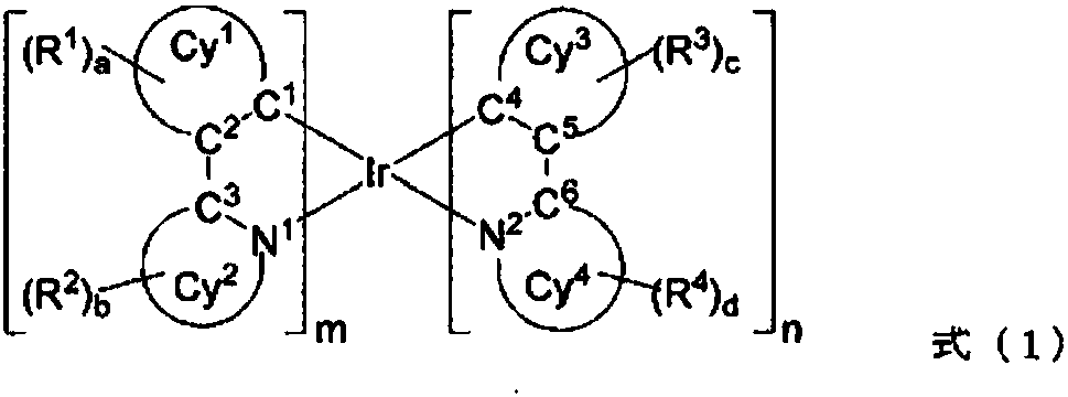
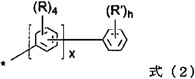
Iridium complex compound, organic electroluminescent element containing said compound, display device and lighting device
A compound, iridium complex technology, applied in the field of iridium complex compounds, can solve the problems of difficult panel enlargement, complicated evaporation process, poor productivity, etc.
- Summary
- Abstract
- Description
- Claims
- Application Information
AI Technical Summary
Problems solved by technology
Method used
Image
Examples
Embodiment
[0330] The following examples are shown to describe the present invention more specifically. However, the present invention is not limited to the following examples, and the present invention can be implemented by arbitrarily changing as long as the gist is not exceeded.
[0331]
[0332] [chemical 18]
[0333] (Synthesis of Intermediate 2)
[0334]
[0335] Under nitrogen flow, 2-(3-pinacolatoborylphenyl)pyridine (17.4 g), Intermediate 1 (19.2 g), 2M aqueous tripotassium phosphate (77 mL), toluene (120 mL) were added to the reaction vessel. ) and ethanol (60 mL), nitrogen was bubbled through for 30 minutes. Thereafter, [Pd(PPh 3 )] 4 (1.21g), stirred and refluxed at 105°C for 1.5 hours. Thereafter, it was cooled to room temperature, and after adding water to perform liquid separation and washing, the organic layer was dried over magnesium sulfate. Thereafter the solvent was removed under reduced pressure. The obtained residue was purified by silica gel column chro...
reference example 1
[0440] Compound D-9, which was synthesized by a method similar to Compound D-1, precipitated rapidly when a 1 wt% solution of phenylcyclohexane adjusted at 100°C was cooled to room temperature. The solubility is very low and cannot be made into ink.
[0441] [chem 46]
[0442]
[0443]
Embodiment 1
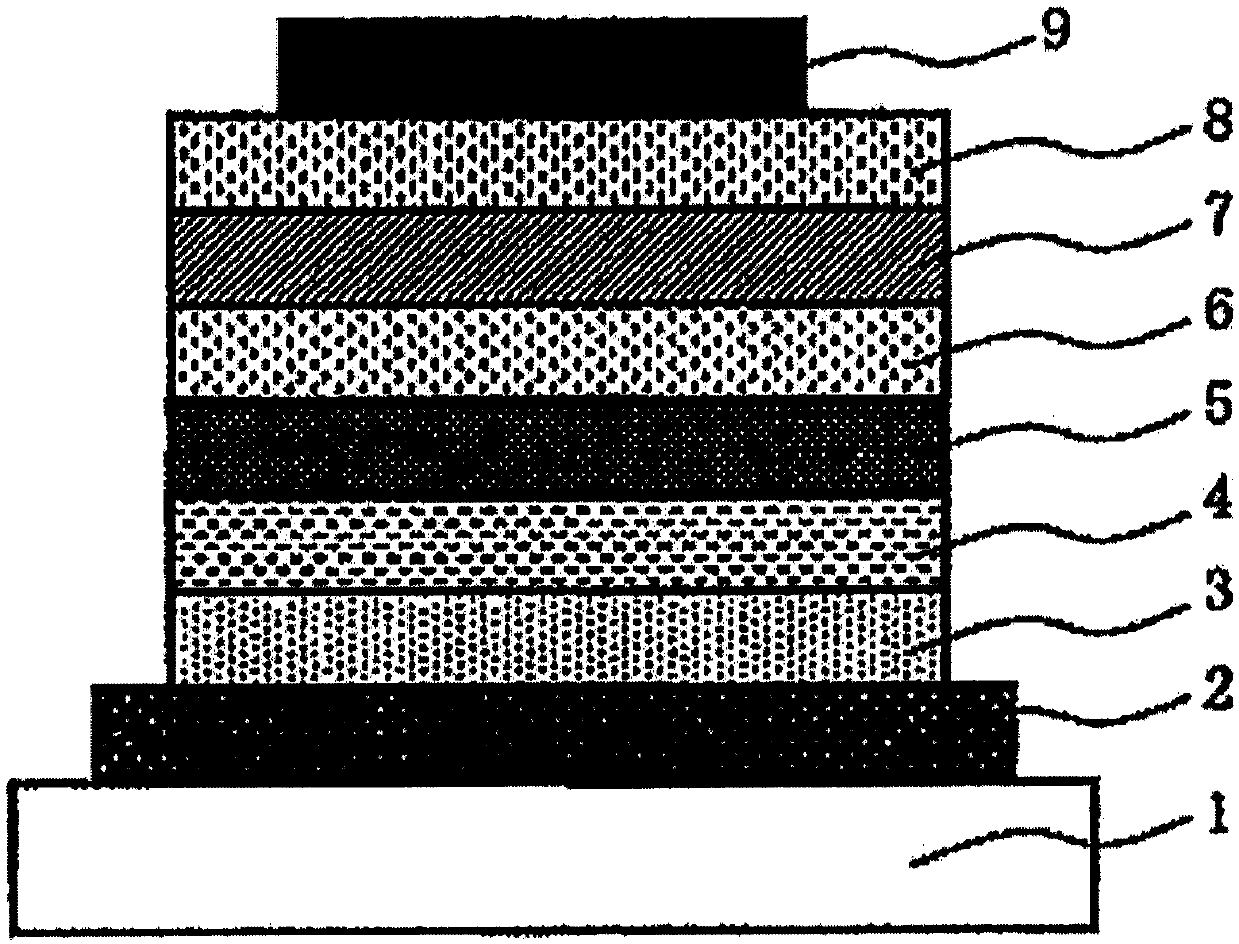
[0446] A product obtained by depositing an indium-tin oxide (ITO) transparent conductive film with a thickness of 70 nm on a glass substrate 1 (manufactured by Geomatec, sputtering film-formed product) was patterned to a width of 2 mm using a common photolithography technique and hydrochloric acid etching. The stripes form the anode 2. The patterned ITO substrate is cleaned in the order of ultrasonic cleaning with aqueous surfactant solution, water washing with ultrapure water, ultrasonic cleaning with ultrapure water, and water washing with ultrapure water, and then dried with compressed air , and finally UV ozone cleaning. This ITO functions as the transparent electrode 2 .
[0447] Next, prepare the arylamine polymer containing the following structural formula (P-1), 4-isopropyl-4'-methyldiphenyliodonium tetrakis(pentafluoro) represented by the structural formula (A-1) A coating solution for forming a hole injection layer of phenyl) borate and ethyl benzoate. This coatin...
PUM
| Property | Measurement | Unit |
|---|---|---|
| Film thickness | aaaaa | aaaaa |
| Film thickness | aaaaa | aaaaa |
| Film thickness | aaaaa | aaaaa |
Abstract
Description
Claims
Application Information
 - R&D
- Intellectual Property
- Life Sciences
- Materials
- Tech Scout
- Unparalleled Data Quality
- Higher Quality Content
- 60% Fewer Hallucinations
Browse by: Latest US Patents, China's latest patents, Technical Efficacy Thesaurus, Application Domain, Technology Topic, Popular Technical Reports.
© 2025 PatSnap. All rights reserved.Legal|Privacy policy|Modern Slavery Act Transparency Statement|Sitemap|About US| Contact US: help@patsnap.com


