Preparation method of cadmium selenide film material
A thin film material, cadmium selenide technology, applied in the field of preparation of cadmium selenide thin film materials, can solve the problems of thin film materials, low compound semiconductor properties, uncontrollable crystal nucleus growth and growth rate, etc., and achieve dislocation density low effect
- Summary
- Abstract
- Description
- Claims
- Application Information
AI Technical Summary
Problems solved by technology
Method used
Image

Examples
Embodiment 1
[0024] Embodiment 1: a kind of preparation method of cadmium selenide film material, concrete steps are:
[0025] (1) Prepare InAs thin film materials on Si substrates by hot wall epitaxy;
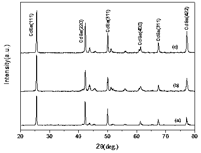
[0026] (2) Put the selenium element and cadmium element into the inner growth tube, put the InAs thin film material obtained in step (1) into the quartz boat, and the quartz boat covers the nozzle of the inner growth tube, and put the inner growth tube and the quartz boat together Push it into the vacuum chamber, vacuumize, and pre-deposit selenium and cadmium on the InAs thin film material to obtain a CdSe buffer layer, wherein the molar ratio of selenium and cadmium is 1:9, and the vacuum degree in the vacuum chamber is 10 -2 The source temperature of Pa, selenium, and cadmium is 330°C, the pre-deposition temperature is 60°C, and the pre-deposition time is 20 min; the surface of the substrate InAs film material has a certain roughness, and the CdSe buffer layer can reduce the generation...
Embodiment 2
[0031] Embodiment 2: a kind of preparation method of cadmium selenide film material, concrete steps are:
[0032] (1) Prepare InAs thin film materials on Si substrates by hot wall epitaxy;
[0033] (2) Put the selenium element and cadmium element into the inner growth tube, put the InAs thin film material obtained in step (1) into the quartz boat, and the quartz boat covers the nozzle of the inner growth tube, and put the inner growth tube and the quartz boat together Push it into the vacuum chamber, vacuumize, and pre-deposit selenium and cadmium on the InAs thin film material to obtain a CdSe buffer layer, wherein the molar ratio of selenium and cadmium is 1:10, and the vacuum degree in the vacuum chamber is 10 -2.5 The source temperature at Pa, selenium, and cadmium is 340°C, the pre-deposition temperature is 61°C, and the pre-deposition time is 25 min; the surface of the substrate InAs film material has a certain roughness, and the CdSe buffer layer can reduce the generat...
Embodiment 3
[0039] Embodiment 3: a kind of preparation method of cadmium selenide film material, concrete steps are:
[0040] (1) Prepare InAs thin film materials on Si substrates by hot wall epitaxy;
[0041] (2) Put the selenium element and cadmium element into the inner growth tube, put the InAs thin film material obtained in step (1) into the quartz boat, and the quartz boat covers the nozzle of the inner growth tube, and put the inner growth tube and the quartz boat together Push it into the vacuum chamber, vacuumize, and pre-deposit selenium and cadmium on the InAs thin film material to obtain a CdSe buffer layer, wherein the molar ratio of selenium and cadmium is 1:11, and the vacuum degree in the vacuum chamber is 10 -3 The source temperature at Pa, selenium, and cadmium is 350°C, the pre-deposition temperature is 62°C, and the pre-deposition time is 30 min; the surface of the substrate InAs film material has a certain roughness, and the CdSe buffer layer can reduce the generatio...
PUM
 Abstract
Description
Claims
Application Information
 - Generate Ideas
- Intellectual Property
- Life Sciences
- Materials
- Tech Scout
- Unparalleled Data Quality
- Higher Quality Content
- 60% Fewer Hallucinations
Browse by: Latest US Patents, China's latest patents, Technical Efficacy Thesaurus, Application Domain, Technology Topic, Popular Technical Reports.
© 2025 PatSnap. All rights reserved.Legal|Privacy policy|Modern Slavery Act Transparency Statement|Sitemap|About US| Contact US: help@patsnap.com