Debugging method and thermal evaporator

A debugging method and evaporation machine technology, which is applied in vacuum evaporation coating, sputtering coating, ion implantation coating, etc., can solve the problems of slow debugging speed, color mixing effect, waste, etc., so as to save organic materials and speed up The effect of debugging speed

Active Publication Date: 2017-12-29
WUHAN CHINA STAR OPTOELECTRONICS SEMICON DISPLAY TECH CO LTD
View PDF6 Cites 1 Cited by
  • Summary
  • Abstract
  • Description
  • Claims
  • Application Information

AI Technical Summary

Problems solved by technology

At present, when the precise mask plate is aligned with the substrate to be operated, the alignment accuracy can usually be controlled within the range of <±3μm, but even if the alignment meets the specification, the actual position of the organic film deposited on the anode pattern of the sub-pixel will be different. Offset, when the organic film or metal film on the anode pattern of the sub-pixel is offset, the color mixing effect will easily occur after the display panel is lit. Therefore, before fully automatic production, the precision mask must be The position is compensated, so that after evaporation and film formation, the film formation pattern covers the sub-pixel anode pattern, and the anode pattern is located in the center of the film formation pattern
[0004] The existing method of adjusting the position of the film-forming pattern of the precision mask plate wastes more film-forming materials, and the debugging speed is relatively slow

Method used


Image

  • Debugging method and thermal evaporator
  • Debugging method and thermal evaporator
  • Debugging method and thermal evaporator

Examples


Embodiment Construction

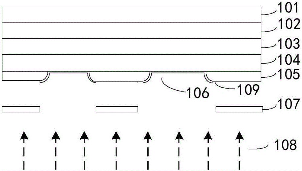
[0025] refer to figure 1 , figure 1 It is a schematic diagram of a debugging substrate and a precision mask plate in the common technology during debugging. The debugging substrate includes: a substrate 101 , a buffer layer 102 , a metal layer 103 , an anode thin film layer 104 and a photoresist layer 105 .

[0026] The substrate 101 is a glass substrate or a substrate having a double-layer structure of a glass substrate and a polyimide film. The material of the buffer layer 102 is silicon nitride or silicon oxide, wherein the buffer layer 102 can be more than one layer, and can be two layers. figure 1 The buffer layer 102 is used as a layer for schematic illustration. The metal layer 103 is a metal molybdenum layer or a multi-layer thin film layer formed of multiple metals, and is used to form an alignment mark of the substrate for debugging. The anode film layer 104 is a multilayer structure formed of indium tin oxide and metal silver. Usually, the anode film layer 104 un...


PUM


Abstract

The invention discloses a debugging method and a thermal evaporator. The method is used for adjusting the relative position of a precise mask plate and a substrate to be operated and includes the steps that the debugging substrate is loaded into a debugging evaporation cavity; the precise mask plate is loaded into the debugging evaporation cavity; a light source in the debugging evaporation cavity is started and further irradiates a photochromic layer on the debugging substrate through the precise mask plate, and the color of the partial region irradiated by irradiation light in the photochromic layer is changed; and the compensation value of the precise mask plate is obtained according to the position of the partial region with the color being changed in the photochromic layer. By adoption of the method, organic materials can be omitted during adjustment, and the debugging speed is increased.

Description

technical field [0001] The invention relates to the field of display technology, in particular to a debugging method and a vapor deposition machine. Background technique [0002] Organic Light Emitting Diode (OLED) display panel has many advantages such as active light emission, high brightness, high contrast ratio, ultra-thin, low power consumption, large viewing angle and wide operating temperature range, and is a new type of flat panel with wide application. display device. [0003] In the process of preparing OLED display panels, it is necessary to use vacuum evaporation technology to prepare OLED thin films. Specifically, organic materials are heated in a vacuum environment, so that the organic materials are sublimated by heat. An organic thin film (also known as a light-emitting layer) with a certain shape is formed on the corresponding anode pattern, in which sub-pixels of different colors correspond to different precision masks, and each color sub-pixel requires a p...

Claims


Application Information

Patent Timeline
Patent Type & Authority Applications(China)
IPC IPC(8): C23C14/04C23C14/24H01L51/56
CPCC23C14/042C23C14/24H10K71/166
Inventor 蒋谦
Owner WUHAN CHINA STAR OPTOELECTRONICS SEMICON DISPLAY TECH CO LTD
Why Eureka
Try Eureka