InGaN-based MSM visible light photoelectric detector with groove-type electrode structure

A photodetector and electrode structure technology, applied in the field of optoelectronics, can solve the problems of epitaxial layer dislocation, phase separation, uneven distribution of In, etc.

Active Publication Date: 2017-12-15
SUN YAT SEN UNIV
View PDF4 Cites 14 Cited by
  • Summary
  • Abstract
  • Description
  • Claims
  • Application Information

AI Technical Summary

Problems solved by technology

The covalent radii of InN and GaN are 1.44 and 1.26 Å respectively, this difference will cause internal stress in InGaN material, and lead to dislocation, phase separation and uneven distribution of In in the epitaxial layer

Method used


Image

  • InGaN-based MSM visible light photoelectric detector with groove-type electrode structure
  • InGaN-based MSM visible light photoelectric detector with groove-type electrode structure
  • InGaN-based MSM visible light photoelectric detector with groove-type electrode structure

Examples


Embodiment 1

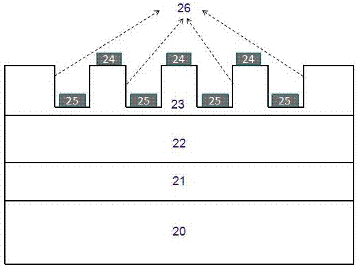
[0028] Such as figure 2 As shown, this method mainly provides an InGaN-based MSM visible light photodetector with a grooved electrode structure. layer, wherein the order of the epitaxial layer from bottom to top is the low-temperature GaN buffer layer 21, the unintentionally doped GaN layer 22, and the unintentionally doped In x Ga 1-x N active layer 23, deposited on In by electron beam evaporation x Ga 1-x The electrode 24 on the N layer 23 and the electrode 25 in the groove 26 . where the unintentional doping of In x Ga 1-x The wavelength range corresponding to the bandgap width in the N layer is 380-780 nm, and the thickness of the InGaN layer is 60-300 nm.

[0029] The process flow includes the following steps:

[0030] (1) Surface cleaning: Place the samples in acetone and isopropanol respectively, and ultrasonically oscillate for organic cleaning, then place the samples in 50% hydrochloric acid to remove the oxide layer on the surface, and dry them with a pure ni...


PUM

PropertyMeasurementUnit
Thicknessaaaaaaaaaa

Abstract

The invention discloses an InGaN-based MSM visible light photoelectric detector with a groove-type electrode structure. The device structure comprises a substrate (10) and an epitaxial layer growing on the substrate (10), wherein the epitaxial layer includes, sequentially from bottom to top, a buffer layer (11), a transition layer (12), an unintentional doping InxGa1-xN active layer (13), and an inserting-finger-shaped electrode (14) and an inserting-finger-shaped electrode (15), which have a schottky metal-semiconductor-metal (MSM) device structure and are coated on an InxGa1-xN active layer (13), wherein the electrode (14) is deposited on the surface of a primordial InxGa1-xN(13), and the electrode (15) is deposited in an inserting-finger-shaped groove (16). The groove (16) is formed on the active layer (13) through etching by a dry method or wet method. Compared with a conventional planar MSM structure, An InGaN-based MSM visible light photoelectric detector with a groove-type electrode structure uses groove sidewall to block leakage current of carriers due to range transition of InGaN original surface, thereby substantially reducing the dark current of the detector. The groove electrode improves the field distribution between electrodes, thereby effectively improving photoelectric current.

Description

technical field [0001] The invention relates to the technical field of optoelectronics, and more specifically, to an InGaN-based MSM visible light photodetector with a grooved electrode structure. Background technique [0002] Visible light communication (Visible Light Communication, VLC) technology is gradually emerging. The Si-based, AlGaAs, and GaP-based detectors used in VLC systems today not only have the problem of low detection sensitivity caused by the inconsistency between the response peak and the main emission wavelength of the light source. Moreover, there are disadvantages of cost increase, volume increase, and filter weakening of the incident optical signal caused by the need for an external optical filter. Although the GaP-based photodetector responds in the visible light band, because it is an indirect bandgap material device, there is a problem of low quantum efficiency. Ternary Compound Semiconductor In x Ga 1-x As a direct bandgap semiconductor material...

Claims


Application Information

Patent Timeline
IPC IPC(8): H01L31/0224H01L31/0304H01L31/108
CPCH01L31/022425H01L31/03044H01L31/108
Inventor 江灏李永贤张晓涵
Owner SUN YAT SEN UNIV
Why Eureka
Try Eureka