
Electro-static discharge circuit waveform detection system and test method

A current waveform and electrostatic discharge technology, which is applied in the field of detection and testing of CDM model electrostatic discharge current waveform, can solve the problems of not specifying the overall structure of the test equipment, lack of accuracy of measurement results, high cost and difficulty in implementation, and reducing measurement technology. Difficulty, easy to build, low testing equipment

Inactive Publication Date: 2017-12-05
SHANGHAI RES INST OF MICROELECTRONICS SHRIME PEKING UNIV
View PDF5 Cites 4 Cited by
  • Summary
  • Abstract
  • Description
  • Claims
  • Application Information

AI Technical Summary

Problems solved by technology

[0006] 1. In the current AEC-Q100 (qualification test process for integrated circuits developed by the AIAG automotive organization) test specification, there is no provision for the overall structure of the test equipment used, as well as related parameters; there is no provision for specific materials , which makes different types of test equipment produced due to different producers in the production process, lacking standardization
At the same time, due to the differences between the various parameters of the various materials that may be used, the measurement results will lack accuracy
[0007] 2. Some foreign companies have produced corresponding CDM model electrostatic discharge test equipment, but this field is still in a blank stage in China
If such non-industrial equipment is required to directly obtain current parameters, the cost and implementation difficulty are high

Method used


Image

  • Electro-static discharge circuit waveform detection system and test method
  • Electro-static discharge circuit waveform detection system and test method
  • Electro-static discharge circuit waveform detection system and test method

Examples


Embodiment

[0028] In an embodiment, the ESD protection current waveform of the CDM model is actually tested.

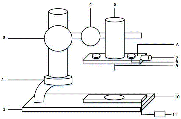
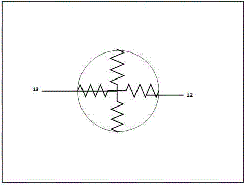
[0029] Place base 1 on a horizontal surface to ensure that the entire test system is level, and then tighten knob 2 to fix the entire upper bracket and base 1 together to prevent movement during testing and adverse effects on measurement results. according to figure 1 After assembling the entire test system as shown, connect the unconnected end of the charging resistor to the positive pole of the DC voltage source, and connect the 8 fixing screws to the negative pole of the DC voltage source. After adjusting the DC voltage source to the required charging voltage, the output voltage is charged to the 10 calibration module through the 11 charging resistor, and the charged 10 calibration module is used to simulate a charged device. Keep the power on, adjust the focus screw 3, and lower the entire bracket until the 9pogo probe touches the copper disc at the center of the calibratio...


PUM

PropertyMeasurementUnit
Thicknessaaaaaaaaaa

Abstract

The present invention provides a CDM (Charged Device Model) current detection system and test method in an ESD (Electro-Static Discharge) electro-static protection. The objective of the invention is to complete the capture of the ESD current waveform of the CDM model so as to facilitate provide data support for ESD electro-static protection taking the CDM as a basis. The system structure comprises a testing machine configured for support, and the pedestal of the machine is provided with a test device DUT (DeviceUnder Test); a machine support is configured to fix the detection module of the system, and the detection module comprises a pogo (pogo stick) probe, a test plate and the like; the testing machine is made of aluminum alloy materials, has a lifting spiral regulation function and is provided with a fixing device capable of fixing the test plate of the device, and the test plate is a dual-layer FR-4 plate; and the pogo probe is a mobile phone antenna special probe capable of satisfying the signal test in the condition of the 18GHz and being less than 18GHz; and the characteristic impedance of a coaxial cable is 50 [Omega], the used calibration module (namely a calibration capacitor) is FR-4 materials, and a capacitance value is 4pF.

Description

technical field [0001] The invention relates to the field of integrated circuits, in particular to a detection and testing method for a CDM model electrostatic discharge current waveform. Background technique [0002] Due to the continuous improvement of the technology level, the size of the Complementary Metal-Oxide-Semiconductor (CMOS, Complementary Metal-Oxide-Semiconductor) device has been in a trend of shrinking, and has reached deep submicron or even smaller. While this development trend improves device performance and working speed, it also brings a fatal weakness, that is, the input impedance is very large, and it is easy to be broken down by Electro-Static Discharge (ESD). [0003] In actual use, there are capacitive effects everywhere. We know that electrostatic charge can be stored in almost all objects, which makes electrostatic discharge appear in various places. At present, for integrated circuits, ESD protection tests can generally be divided into HBM (Human...

Claims


Application Information

Patent Timeline
IPC IPC(8): G01R23/16G01R13/00
CPCG01R23/16G01R13/00
Inventor 陈昭程玉华
Owner SHANGHAI RES INST OF MICROELECTRONICS SHRIME PEKING UNIV
Learn More