Micro heating plate based on porous silicon insulation layer and preparation method thereof
A porous silicon layer and micro-heating technology, which is applied in ohmic resistance heating, heating element materials, ohmic resistance heating parts, etc., can solve the problems of complex process and various manufacturing processes, and achieve low cost, uniform temperature distribution, large The effect of contact area
- Summary
- Abstract
- Description
- Claims
- Application Information
AI Technical Summary
Problems solved by technology
Method used
Image
Examples
Embodiment 1
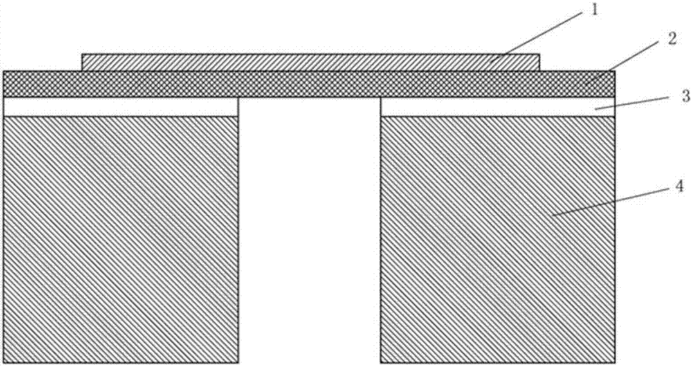
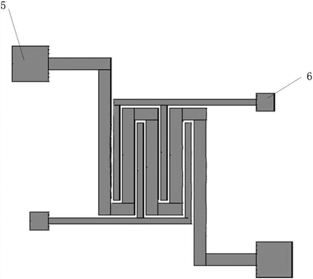
[0035] A micro-heating plate based on a porous silicon thermal insulation layer, the heating plate adopts a multilayer structure, refer to figure 1 , From top to bottom including electrode group 1, porous silicon layer 2, silicon dioxide layer 3 and silicon base 4, said electrode group 1 includes heating electrode 5 and signal electrode 6, refer to figure 2 , The heating electrode 5 has a serpentine shape, the signal electrode 6 is an interdigital electrode, the signal electrode 6 is arranged in a serpentine depression of the heating electrode 5, and the heating electrode 5 and the signal electrode 6 are mutually not in contact. The electrode group 1 has a thickness of 35 μm, the porous silicon layer 2 has a thickness of 100 μm, the silicon dioxide layer 3 has a thickness of 35 μm, and the silicon base 4 has a thickness of 1.8 mm.
[0036] The silicon base 4 options For single crystal silicon, a silicon dioxide layer 3 is provided on the upper surface of the silicon base 4 to su...
Embodiment 2
[0044] A micro-heating plate based on a porous silicon thermal insulation layer, the heating plate adopts a multilayer structure, refer to figure 1 , From top to bottom including electrode group 1, porous silicon layer 2, silicon dioxide layer 3 and silicon base 4, said electrode group 1 includes heating electrode 5 and signal electrode 6, refer to figure 2 , The heating electrode 5 has a serpentine shape, the signal electrode 6 is an interdigital electrode, the signal electrode 6 is arranged in a serpentine depression of the heating electrode 5, and the heating electrode 5 and the signal electrode 6 are mutually not in contact. The thickness of the electrode group 1 is 45 μm, the thickness of the porous silicon layer 2 is 110 μm, the thickness of the silicon dioxide layer 3 is 45 μm, and the thickness of the silicon base 4 is 2.2 mm.
[0045] The silicon base 4 options For single crystal silicon, a silicon dioxide layer 3 is provided on the upper surface of the silicon base 4 t...
Embodiment 3
[0053] A micro-heating plate based on a porous silicon thermal insulation layer, the heating plate adopts a multilayer structure, refer to figure 1 , From top to bottom including electrode group 1, porous silicon layer 2, silicon dioxide layer 3 and silicon base 4, said electrode group 1 includes heating electrode 5 and signal electrode 6, refer to figure 2 , The heating electrode 5 has a serpentine shape, the signal electrode 6 is an interdigital electrode, the signal electrode 6 is arranged in a serpentine depression of the heating electrode 5, and the heating electrode 5 and the signal electrode 6 are mutually not in contact. The thickness of the electrode group 1 is 40 μm, the thickness of the porous silicon layer 2 is 110 μm, the thickness of the silicon dioxide layer 3 is 40 μm, and the thickness of the silicon base 4 is 2 mm.
[0054] The silicon base 4 options For single crystal silicon, a silicon dioxide layer 3 is provided on the upper surface of the silicon base 4 to ...
PUM
| Property | Measurement | Unit |
|---|---|---|
| thickness | aaaaa | aaaaa |
| thickness | aaaaa | aaaaa |
| thickness | aaaaa | aaaaa |
Abstract
Description
Claims
Application Information
 - R&D
- Intellectual Property
- Life Sciences
- Materials
- Tech Scout
- Unparalleled Data Quality
- Higher Quality Content
- 60% Fewer Hallucinations
Browse by: Latest US Patents, China's latest patents, Technical Efficacy Thesaurus, Application Domain, Technology Topic, Popular Technical Reports.
© 2025 PatSnap. All rights reserved.Legal|Privacy policy|Modern Slavery Act Transparency Statement|Sitemap|About US| Contact US: help@patsnap.com


