
Fast dark-field detection method for surface microdefects of large-caliber fused quartz optical element

An optical element and dark field detection technology, applied in the field of engineering optics, can solve the problems of low detection accuracy and efficiency, limited acquisition frame rate, and reduced scanning efficiency, so as to save rapid detection time, improve detection efficiency, and improve detection. The effect of precision

Active Publication Date: 2017-11-17
LASER FUSION RES CENT CHINA ACAD OF ENG PHYSICS +1
View PDF8 Cites 21 Cited by
  • Summary
  • Abstract
  • Description
  • Claims
  • Application Information

AI Technical Summary

Problems solved by technology

The visual inspection method is limited by the proficiency of the operator. Each inspection will be subject to a certain degree. Long-term operation will cause eye fatigue. At the same time, the size and location information of the detected micro-defects cannot be accurately quantified. low efficiency
With the development of technology, there has been a method of using an area array CCD camera to scan the surface of the fused silica optical element for full-aperture scanning detection, which improves the accuracy of detection, and performs data processing on the acquired micro-defect images to extract micro-defects The information characteristics can realize the accurate quantification of micro-defect information, but limited by the acquisition frame rate of the area array CCD camera, the scanning speed needs to be kept in a low range, which greatly reduces the scanning efficiency

Method used


Image

  • Fast dark-field detection method for surface microdefects of large-caliber fused quartz optical element
  • Fast dark-field detection method for surface microdefects of large-caliber fused quartz optical element
  • Fast dark-field detection method for surface microdefects of large-caliber fused quartz optical element

Examples


Embodiment Construction

[0043] The present invention will be further described in detail below in conjunction with the accompanying drawings, so that those skilled in the art can implement it with reference to the description.

[0044] It should be understood that terms such as "having", "comprising" and "including" as used herein do not entail the presence or addition of one or more other elements or combinations thereof.

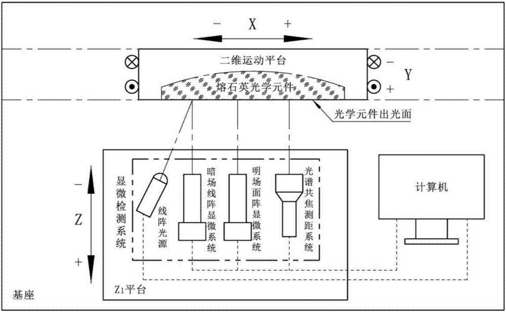
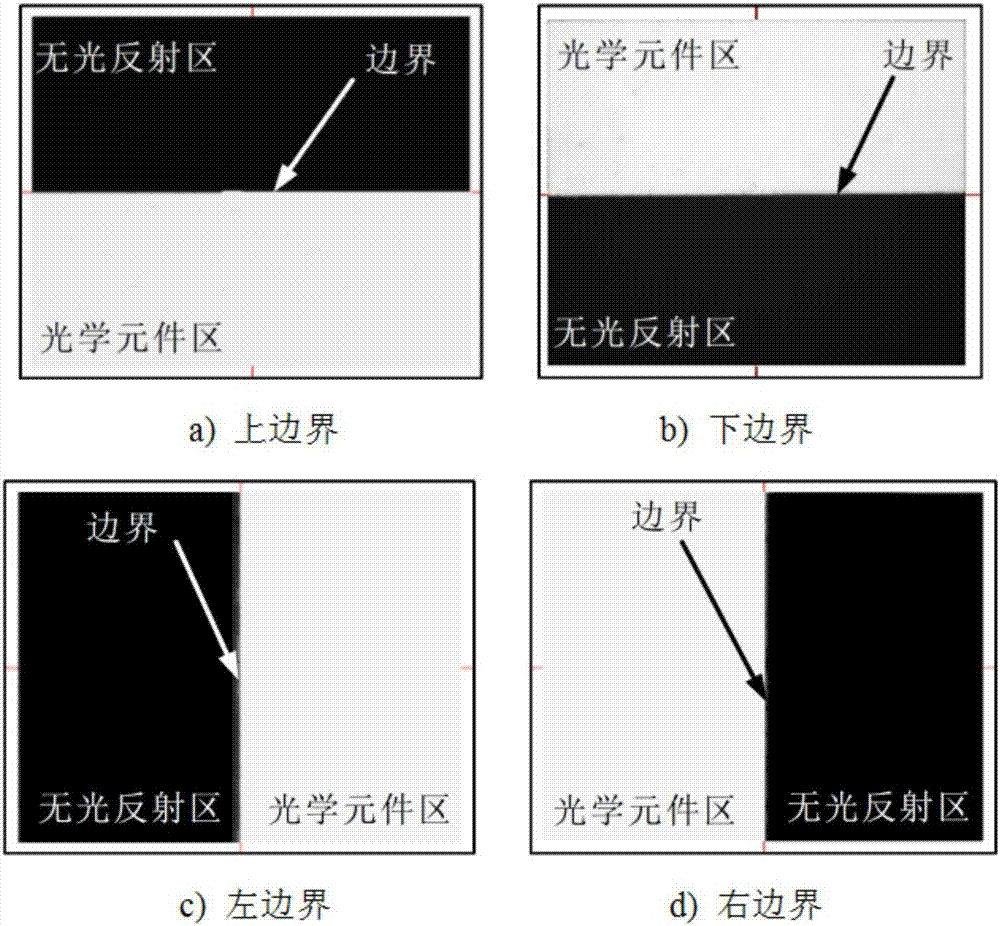
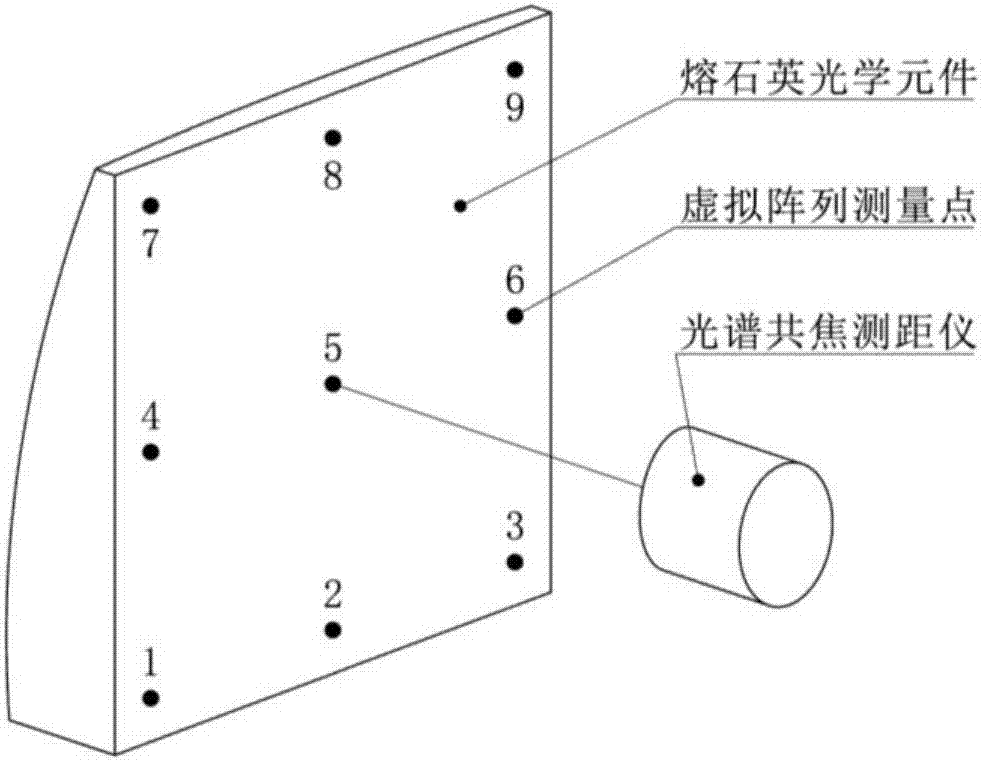
[0045] The invention discloses a fast dark-field detection method for micro-defects on the surface of a large-diameter fused silica optical element. Firstly, a bright-field array CCD microscope system is used to locate the optical element, and the position of the optical element in an absolute coordinate system is determined, and then the spectral The confocal distance measuring system determines the light surface equation of the optical element irradiated by strong laser light. Finally, the dark field linear array CCD microscope system is used to scan the surface of the precisely...


PUM


Abstract

The invention discloses a fast dark-field detection method for surface microdefects of a large-caliber fused quartz optical element. The method includes the steps that firstly, a bright-field area array CCD microscope system is adopted to position the optical element so as to determine the position of the optical element in an absolute coordinate system; then, a spectral confocal ranging system is adopted to determine a high-intensity laser irradiation light-outlet surface equation of the optical element; finally, a dark-field linear array CCD microscope system is adopted to conduct one-way line-by-line fast raster scanning on the surface of the large-caliber fused quartz optical element moving precisely so as to obtain microdefect information, and the bright-field area array CCD microscope system is adopted to monitor the optical element on line. By means of the method, full-caliber automatic scanning for surface microdefects of the optical element is achieved, the detection efficiency is greatly improved, and the full-caliber fast scanning and detecting time for surface microdefects of the optical element can be controlled within 30 min.

Description

technical field [0001] The invention belongs to the field of engineering optics, and in particular relates to a fast dark-field detection method for micro-defects on the surface of a large-diameter fused silica optical element. Background technique [0002] Large-aperture fused silica optical components are the most commonly used optical components in the terminal optical components of high-power solid-state laser devices. Surface micro-defects, especially in high-power solid-state laser systems, when large-aperture fused silica optical elements are irradiated by triple-frequency ultraviolet strong lasers, micro-cracks, micro-pits and other ablation point micro-defects are more likely to occur. When micro-defects such as micro-cracks or micro-pits appear at ablation points, the light transmission performance and thermodynamic properties of optical components will be weakened, which seriously affects the energy flux density of strong laser output and the service life of optic...

Claims


Application Information

Patent Timeline
IPC IPC(8): G01N21/95
CPCG01N21/95G01N2021/9511
Inventor 袁晓东赵林杰程健陈明君廖威王海军张传超陈静张丽娟
Owner LASER FUSION RES CENT CHINA ACAD OF ENG PHYSICS
Learn More