
Dielectric metasurface collimating lens matched with terahertz photoconductive antenna in use

A technology of photoconductive antenna and collimating lens is applied in the field of dielectric metamaterials in the terahertz band, which can solve the problems of miniaturization, occupied space, large refractive index of silicon, etc. , the effect of high transmittance

Inactive Publication Date: 2017-11-03
TIANJIN UNIV
View PDF3 Cites 16 Cited by
  • Summary
  • Abstract
  • Description
  • Claims
  • Application Information

AI Technical Summary

Problems solved by technology

The terahertz wave passes through the super-hemispheric high-resistance silicon lens and finally diverges at a cone angle of 34° [4] , the parabolic mirror or terahertz lens is needed to converge the terahertz wave again in order to collimate the terahertz wave into a plane wave. Since the parabolic mirror and terahertz lens occupy a certain amount of space, this will not be conducive to the realization of a small terahertz system. change
Usually, the hyperhemispherical high-resistance silicon lens used in the terahertz time-domain spectroscopy system has a diameter of about 1 cm. Due to the spherical shape of the hyperhemispherical silicon lens, it cannot be directly grown on the antenna by photolithography. Antenna alignment and installation issues
The more important problem is that the refractive index of silicon is too large, and the reflection loss of terahertz waves is serious at the silicon-air interface

Method used


Image

  • Dielectric metasurface collimating lens matched with terahertz photoconductive antenna in use
  • Dielectric metasurface collimating lens matched with terahertz photoconductive antenna in use
  • Dielectric metasurface collimating lens matched with terahertz photoconductive antenna in use

Examples


Embodiment Construction

[0026] The existing hyperhemispheric silicon lens used in conjunction with the terahertz emitting photoconductive antenna can achieve the convergence of the terahertz wave, which has the advantages of no dispersion and low absorption, but its collimation effect on the terahertz wave is not ideal. It needs to be used together with a parabolic mirror or a terahertz lens to collimate the terahertz optical path into a quasi-parallel beam. The silicon lens itself is a bulk material, and the introduction of the parabolic mirror and the terahertz lens makes the integration of the whole system Very low, cumbersome and cumbersome, which is not conducive to the flexible use of the terahertz system, thus limiting the application of the terahertz system. The hyperhemispherical high-resistance silicon lens used in the terahertz time-domain spectroscopy system has a diameter of about 1 cm. Such a large-sized hyperhemispherical silicon lens requires precise machining and polishing processes, ...


PUM

PropertyMeasurementUnit
Thicknessaaaaaaaaaa
Thicknessaaaaaaaaaa
Heightaaaaaaaaaa

Abstract

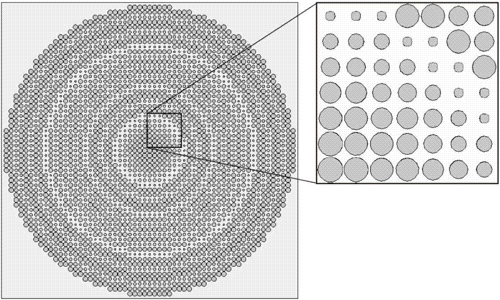
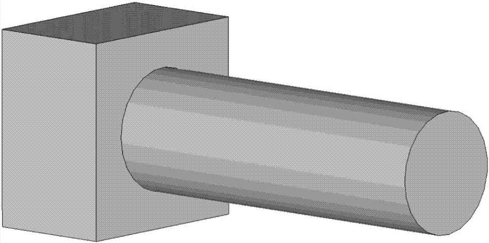
The invention relates to a terahertz waveband dielectric metamaterial, and aims to design and produce a device with a small size, easy integration and higher transmission efficiency for improving the flexibility of a photoconductive antenna-based terahertz time-domain spectral system, so as to replace a silicon lens and a paraboloidal mirror or a silicon lens and a terahertz lens. A technical scheme is adopted as follows: a dielectric metasurface collimating lens matched with a terahertz photoconductive antenna in use consists of two parts: a substrate layer and a two-dimensional microstructure layer, wherein the substrate layer is an isotropous high-resistance silicon layer with uniform thickness; the substrate layer is used for providing mechanical support for the two-dimensional microstructure layer, and the two-dimensional microstructure layer is also made from high-resistance silicon; the two-dimensional microstructure layer is formed by tetragonal lattices of cylindrical structures in arrangement similar to a concentric annulus way; and the cylindrical structures of different diameters have different modulation depths on phases, and the cylindrical structures on the same ring of the concentric annulus are the same in diameters. The dielectric metasurface collimating lens is mainly applied to design and manufacturing of the device with higher transmission efficiency.

Description

technical field [0001] The invention relates to a dielectric metamaterial in the terahertz band, which can be used in a terahertz system with a planar photoconductive antenna emission source instead of a traditional super-hemispheric high-resistance silicon lens to realize the collimation of terahertz waves. Specifically, it involves a dielectric metasurface collimating lens used in conjunction with a terahertz photoconductive antenna. Background technique [0002] In recent years, terahertz technology has become a research hotspot in the fields of electromagnetics and spectroscopy. Terahertz science and technology integrates the characteristics of electronics and photonics, involving physics, chemistry, optics, material science, microwave and millimeter wave electronics and other disciplines, and is a typical interdisciplinary frontier discipline. Compared with infrared waves, terahertz waves have less scattering and stronger penetrating power. Compared with microwaves, te...

Claims


Application Information

Patent Timeline
IPC IPC(8): H01Q15/08
Inventor 谷建强余晴许悦红欧阳春梅田震韩家广张伟力
Owner TIANJIN UNIV
Learn More