
A method of fabricating a selectively doped structure

A selective, matrix technology, applied in the field of solar cells, can solve problems such as difficult mass production, large damage to silicon wafers, and surface concentration in lightly doped regions, so as to reduce surface recombination and emitter layer recombination, improve open circuit voltage and Short-circuit current, the effect of improving the quantum response

Active Publication Date: 2019-06-11
TAIZHOU ZHONGLAI PHOTOELECTRIC TECH CO LTD
View PDF5 Cites 0 Cited by
  • Summary
  • Abstract
  • Description
  • Claims
  • Application Information

AI Technical Summary

Problems solved by technology

Among them, the two-step diffusion method needs to go through two high-temperature processes, which will cause great damage to the silicon wafer. At the same time, the process is complicated and difficult to mass-produce; the laser doping method is difficult to obtain the square resistance of the low heavily doped area and the surface of the low lightly doped area at the same time. Concentration; Phosphorus slurry diffusion method is difficult to control the outdiffusion effect of phosphorus slurry at high temperature, this kind of outdiffusion will affect the quality of lightly doped region junctions, and this method cannot eliminate the pollution caused by the phosphorus slurry itself and the process
Although the reverse etch-back method can obtain a lower surface concentration of the lightly doped region, it is difficult to control the uniformity of the square resistance of the lightly doped region. At the same time, this method involves the printing and removal of the mask, which will increase the cost of auxiliary materials and production

Method used


Image

  • A method of fabricating a selectively doped structure
  • A method of fabricating a selectively doped structure
  • A method of fabricating a selectively doped structure

Examples


Embodiment 1

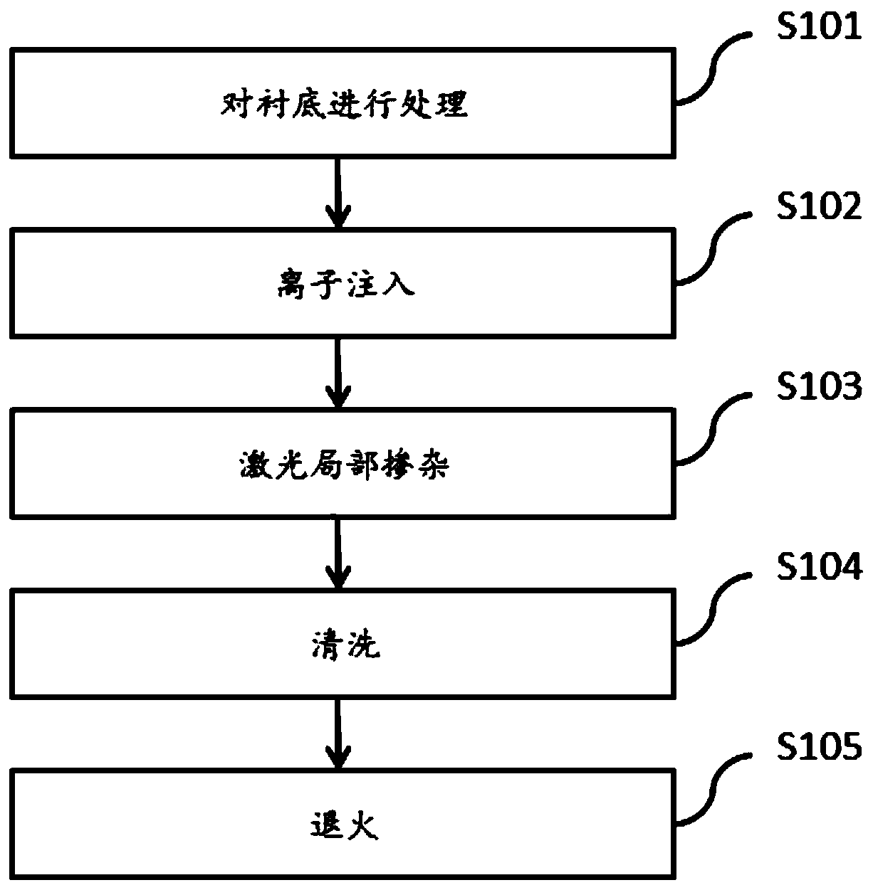
[0034] see Figure 1 to Figure 5 As shown, a method for fabricating a selectively doped structure provided in this embodiment includes the following steps:

[0035] S101. Select a P-type crystalline silicon substrate 10 of 156mm*156mm, and perform texturing and cleaning treatment on the surface of the P-type crystalline silicon substrate 10; the resistivity of the P-type crystalline silicon substrate 10 is 0.5-15Ω·cm, preferably 1~ 5Ω·cm; the thickness of the P-type crystalline silicon substrate 10 is 50-300 μm, preferably 80-200 μm.

[0036] S102. Use an ion implanter to perform ion implantation on the front surface of the P-type crystalline silicon substrate 10 processed in step S101. The implanted element is phosphorus, and the implantation dose is 0.5×10 15 cm -2 ~3×10 15 cm -2 , preferably 1.5×10 15 cm -2 ~2.5×10 15 cm -2 . After the implantation is completed, a phosphorus-doped amorphous silicon layer 13 is formed on the front surface of the P-type crystalline s...

Embodiment 2

[0048] see Figure 1 to Figure 5 As shown, a method for fabricating a selectively doped structure provided in this embodiment includes the following steps:

[0049] S101. Select an N-type crystalline silicon substrate 10 of 156mm*156mm, and perform texturing and cleaning treatment on the surface of the N-type crystalline silicon substrate 10; the resistivity of the N-type crystalline silicon substrate 10 is 0.5-15Ω·cm, preferably 1- 5Ω·cm; the thickness of the N-type crystalline silicon substrate 10 is 50-300 μm, preferably 80-200 μm.

[0050] S102. Use an ion implanter to perform ion implantation on the back surface of the N-type crystalline silicon substrate 10 processed in step S101. The implanted element is phosphorus, and the implantation dose is 0.5×10 15 cm -2 ~3×10 15 cm -2 , preferably 1.5×10 15 cm -2 ~2.5×10 15 cm -2 . After the implantation is completed, a phosphorus-doped amorphous silicon layer 13 is formed on the back surface of the N-type crystalline si...

Embodiment 3

[0054] see Figure 1 to Figure 5 As shown, a method for fabricating a selectively doped structure provided in this embodiment includes the following steps:

[0055] S101. Select an N-type crystalline silicon substrate 10 of 156mm*156mm, and perform texturing and cleaning treatment on the surface of the N-type crystalline silicon substrate 10; the resistivity of the N-type crystalline silicon substrate 10 is 0.5-15Ω·cm, preferably 1- 5Ω·cm; the thickness of the N-type crystalline silicon substrate 10 is 50-300 μm, preferably 80-200 μm.

[0056] S102. Use an ion implanter to perform ion implantation on the front surface of the N-type crystalline silicon substrate 10 processed in step S101. The implanted element is boron, and the implantation dose is 0.5×10 15 cm -2 ~3×10 15 cm -2 , preferably 1.5×10 15 cm -2 ~2.5×10 15 cm -2 . After the implantation is completed, a boron-doped amorphous silicon layer 13 is formed on the back surface of the N-type crystalline silicon sub...


PUM

PropertyMeasurementUnit
electrical resistivityaaaaaaaaaa
thicknessaaaaaaaaaa
thicknessaaaaaaaaaa

Abstract

The invention relates to a method for manufacturing a selective doping structure. The method comprises the following steps of subjecting a silicon substrate to surface texturing and cleaning treatment; carrying out the ion implantation on the surface of the silicon substrate; subjecting the ion implantation surface of the silicon substrate to laser local treatment to form a heavily doped region; subjecting the silicon substrate to cleaning treatment after the injection treatment of the silicon substrate; forming a lightly doped region by high-temperature annealing, reconstructing the heavily doped region, and finally preparing the selective doping structure. The method is simple in process, and only one step of laser local treatment is added compared with the whole-surface uniform doping process based on ion implantation. Compared with other methods for manufacturing selective doping structures, the heavily doped region of the above method is larger in junction depth, and a prepared battery is small in reverse electricity leakage and high in parallel resistance. The cleaning treatment is conducted after the injection treatment, so that a lightly doped region of a low surface concentration is formed after the annealing treatment. Therefore, the open-circuit voltage and the short-circuit current of the prepared battery are improved. A more uniform doping amount can be obtained through ion implantation, and the square resistance uniformity of the lightly doped region is good.

Description

technical field [0001] The invention relates to the technical field of solar cells, in particular to a method for making a selective doping structure. Background technique [0002] A solar cell is a semiconductor device that converts solar energy into electricity. In conventional crystalline silicon solar cells, in order to reduce the contact resistance between electrodes and silicon wafers, it is generally required to control the sheet resistance below 100Ω / sqr. conversion efficiency limitation. Selective emitter solar cells can solve this problem well. [0003] The main feature of selective emitter solar cells is high doping concentration in the metallized area and low doping concentration in the illuminated area. Composite to improve the quantum response and battery performance in the blue light band. Selective diffusion solar cells have a good gold-half ohmic contact; the metallization area is thick and the diffusion area has a deep junction, and impurities such as m...

Claims


Application Information

Patent Timeline
Patent Type & Authority Patents(China)
IPC IPC(8): H01L31/18H01L21/02H01L21/268
CPCH01L21/02057H01L21/268H01L31/1804Y02P70/50
Inventor 林建伟王建明吴兴华季根华刘志锋刘勇
Owner TAIZHOU ZHONGLAI PHOTOELECTRIC TECH CO LTD
Learn More