A kind of infrared LED and preparation method thereof
An infrared and epitaxial layer technology, applied in semiconductor devices, electrical components, circuits, etc., can solve the problems of limiting the performance of PINGeSn light-emitting tubes, high dislocation density of Ge epitaxial layers, large surface roughness, etc. Avoid unintentional doping, high quality results
- Summary
- Abstract
- Description
- Claims
- Application Information
AI Technical Summary
Problems solved by technology
Method used
Image

Examples
Embodiment 1
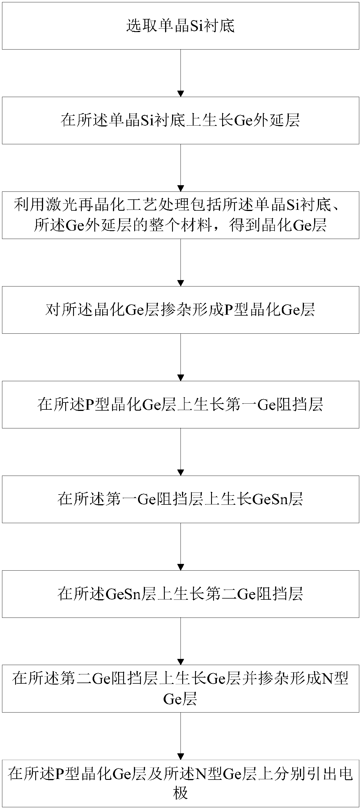
[0051] See figure 1 , figure 1 A flow chart of a method for preparing an infrared LED provided in an embodiment of the present invention, wherein the method includes:
[0052] (a) select a single crystal Si substrate;
[0053] (b) growing a Ge epitaxial layer on the single crystal Si substrate;
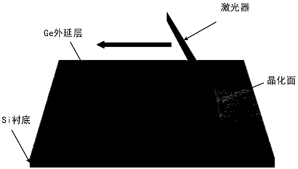
[0054] (c) processing the entire material including the single crystal Si substrate and the Ge epitaxial layer by a laser recrystallization process to obtain a crystallized Ge layer;
[0055] (d) doping the crystallized Ge layer to form a p-type crystallized Ge layer;
[0056] (e) growing a first Ge barrier layer on the p-type crystallized Ge layer;
[0057] (f) growing a GeSn layer on the first Ge barrier layer;
[0058] (g) growing a second Ge barrier layer on the GeSn layer;
[0059] (h) growing a Ge layer on the second Ge barrier layer and doping to form an N-type Ge layer;
[0060] (i) Drawing out electrodes on the P-type crystallized Ge layer and the N-type Ge layer respe...
Embodiment 2
[0096] Please refer to Figure 3a-Figure 3m , Figure 3a-Figure 3m It is a schematic diagram of a preparation method of an infrared LED according to an embodiment of the present invention, and the preparation method includes the following steps:
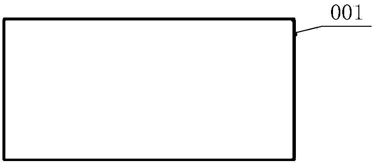
[0097] S101, select single crystal Si substrate 001, such as Figure 3a shown.
[0098] S102. At a temperature of 250° C. to 350° C., a Ge seed layer 002 of 40 to 50 nm is grown on a single crystal Si substrate 001 by using a CVD process, such as Figure 3b shown.
[0099] S103, at a temperature of 550° C. to 600° C., using a CVD process to grow a Ge main layer 003 with a thickness of 150 to 250 nm on the surface of the Ge seed layer 002, such as Figure 3c shown.
[0100] S104, growing SiO with a thickness of 100-150 nm on the surface of the Ge main body layer 003 by using a CVD process 2 protective layer 004, such as Figure 3d shown.
[0101] S105, heating the entire substrate material including the single crystal Si subst...
Embodiment 3
[0112] Please refer to Figure 4 , Figure 4 It is a schematic structural diagram of an infrared LED provided by an embodiment of the present invention. The luminous tube adopts the above-mentioned Figure 3a-Figure 3m prepared as indicated. Specifically, the LED comprises: a single crystal Si substrate 301, a P-type crystallized Ge layer 302, a first Ge barrier layer 303, a GeSn layer 304, a second Ge barrier layer 305, an N-type Ge layer 306, a SiO 2 Passivation layer 307 and Cr—Au alloy electrode 308 .
PUM
| Property | Measurement | Unit |
|---|---|---|
| thickness | aaaaa | aaaaa |
| thickness | aaaaa | aaaaa |
| thickness | aaaaa | aaaaa |
Abstract
Description
Claims
Application Information
 - R&D
- Intellectual Property
- Life Sciences
- Materials
- Tech Scout
- Unparalleled Data Quality
- Higher Quality Content
- 60% Fewer Hallucinations
Browse by: Latest US Patents, China's latest patents, Technical Efficacy Thesaurus, Application Domain, Technology Topic, Popular Technical Reports.
© 2025 PatSnap. All rights reserved.Legal|Privacy policy|Modern Slavery Act Transparency Statement|Sitemap|About US| Contact US: help@patsnap.com