
Method of making back-hole mask of 6-inch-substrate-based GaN device

A manufacturing method and back hole technology, applied in semiconductor/solid-state device manufacturing, semiconductor devices, electrical components, etc., can solve problems such as high cost, unsuitable for batch production, and long time consumption, so as to improve utilization rate and reduce machine time , Reduce the effect of process steps

Active Publication Date: 2017-09-01
CHENGDU HIWAFER SEMICON CO LTD
View PDF2 Cites 2 Cited by
  • Summary
  • Abstract
  • Description
  • Claims
  • Application Information

AI Technical Summary

Problems solved by technology

This method is not only time-consuming, but also costly. It usually takes about 5 hours for sputtering, which is really not suitable for mass production.

Method used


Image

  • Method of making back-hole mask of 6-inch-substrate-based GaN device

Examples


Embodiment Construction

[0023] The following will clearly and completely describe the technical solutions in the embodiments of the present invention with reference to the accompanying drawings in the embodiments of the present invention. Obviously, the described embodiments are only some, not all, embodiments of the present invention. Based on the embodiments of the present invention, all other embodiments obtained by persons of ordinary skill in the art without making creative efforts belong to the protection scope of the present invention.

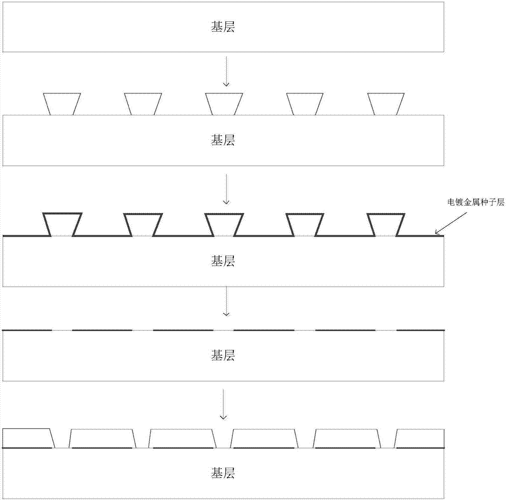
[0024] see figure 1 A method for manufacturing a backhole mask based on a 6-inch GaN device is provided, including the following steps:

[0025] Step 1: Rinse the particles and foreign matter on the surface of the wafer with a developer, make a photoresist arc island with a back hole shape of 2 μm in thickness and 80 μm in diameter, and transfer the pattern on the mask plate to the cover by photolithography On the wafer with photoresist, the photolithography ...


PUM

PropertyMeasurementUnit
thicknessaaaaaaaaaa

Abstract

The invention relates to a method of making a back-hole mask of a 6-inch-substrate-based GaN device. In order to solve problems in the traditional GaN HEMT device manufacturing process, the invention provides a novel method for making a back-hole mask in a 6-inch-substrate-based GaN / SiC device. A metal nickel material is prepared by means of photoetching, sputtering, peeling and electroplating to realize SiC mask etching. The metal Ni has the thickness of 10 microns, the uniformity less than or equal to 5%, and the side wall angle larger than 60 degrees; and the diameter of the back hole is but not limited to 60 microns.

Description

technical field [0001] The invention relates to a method for manufacturing a backhole mask based on a 6-inch GaN device, belonging to the field of integrated circuit manufacturing. Background technique [0002] GaN high electron mobility transistor (HEMT) devices have the advantages of very high two-dimensional electron gas (2-DEG) concentration, high saturation electron mobility, high breakdown voltage and high power density, making GaN HEMT devices not only in the known Microwave power applications have advantages that GaAs devices cannot match, and they also have the same advantages in new low-noise applications, such as: better linearity, higher dynamic range under the same noise figure; Large broadband characteristics, suitable for ultra-wideband devices; can withstand higher burnout input power, can increase the anti-interference ability of the whole machine, and simplify the front-end protection circuit. Therefore, GaN HEMT low-noise devices and their monolithic inte...

Claims


Application Information

Patent Timeline
Patent Type & Authority Applications(China)
IPC IPC(8): H01L21/033H01L21/04H01L21/335
CPCH01L21/0337H01L21/0475H01L29/66462
Inventor 王珺楠
Owner CHENGDU HIWAFER SEMICON CO LTD
Learn More