A kind of lateral structure germanium/silicon heterojunction avalanche photodetector and preparation method thereof
An avalanche photoelectric and silicon heterojunction technology, applied in photovoltaic power generation, circuits, electrical components, etc., can solve the problems of difficult preparation, high doping control requirements, complex structure of avalanche photodetectors, etc., and achieve easy preparation , good consistency and simple structure
- Summary
- Abstract
- Description
- Claims
- Application Information
AI Technical Summary
Problems solved by technology
Method used
Image
Examples
Embodiment 1
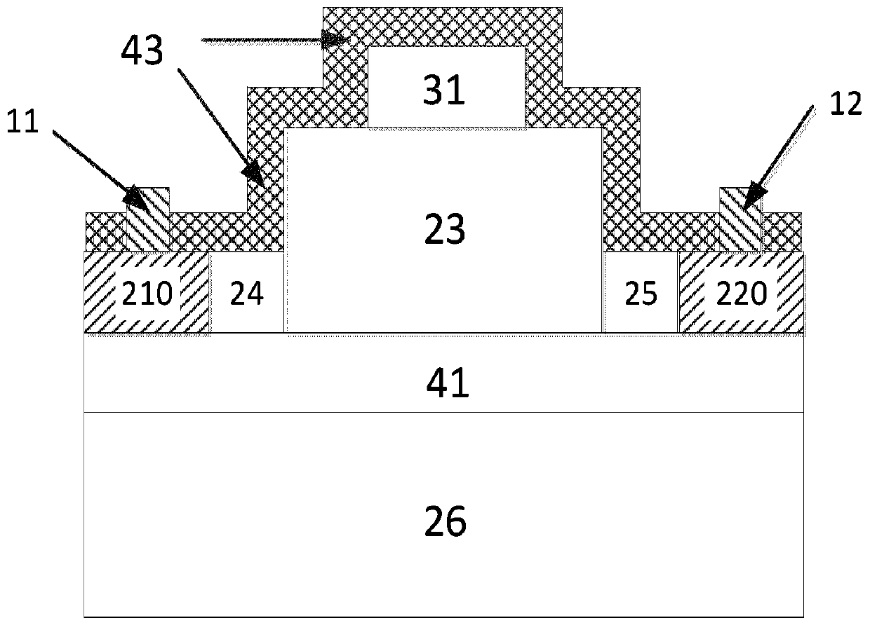
[0045] Example 1 as figure 1 Shown is a lateral structure germanium / silicon heterojunction avalanche photodetector provided by an embodiment of the present invention, including: a positive electrode 11, a negative electrode 12, a silicon P + Contact region 210, silicon N + Contact region 220 , silicon mesa region 23 , first silicon space region 24 , second silicon space region 25 , germanium epitaxial layer 31 , surface passivation layer 43 , buried silicon oxide 41 and silicon substrate 26 .
[0046] The silicon substrate 26 and the buried silicon oxide 41 are made of SOI material, and the buried silicon oxide 41 is formed on the silicon substrate 26 . The silicon mesa region 23 is formed on the buried silicon oxide 41 by etching the surface device silicon layer on the buried silicon oxide 41 .
[0047] The first silicon space region 24 and the second silicon space region 25 are respectively formed on the buried silicon oxide 41 on both sides of the silicon mesa region 23 ,...
Embodiment 2
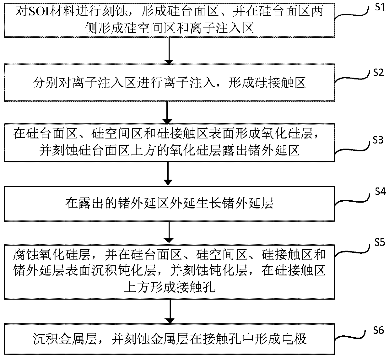
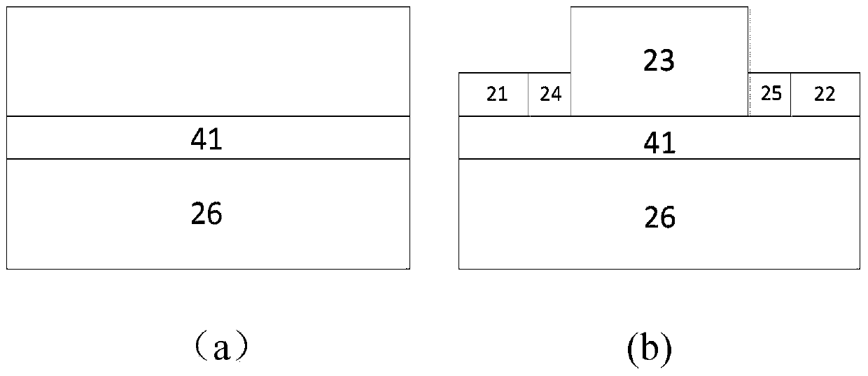
[0057] figure 2 The flow chart of the steps of a method for preparing a lateral structure germanium / silicon heterojunction avalanche photodetector provided by the patent embodiment of the present invention, image 3 A schematic diagram of the structure during device fabrication is given, corresponding to the following implementation steps. Combine below figure 2 and image 3 Introduce the preparation method of the device:
[0058] Step S1: Etching the SOI material to form a silicon mesa region, and forming silicon space regions and ion implantation regions on both sides of the silicon mesa region.
[0059] Such as image 3 As shown in (a), the preparation starts from the SOI material, which has a three-layer structure, including a stacked substrate 26 , buried silicon oxide 41 , and a surface device silicon layer above the buried silicon oxide 41 .
[0060] First, the SOI material is cleaned by organic and inorganic solvents. If the SOI material has a good clean packag...
PUM
 Abstract
Description
Claims
Application Information
 - R&D
- Intellectual Property
- Life Sciences
- Materials
- Tech Scout
- Unparalleled Data Quality
- Higher Quality Content
- 60% Fewer Hallucinations
Browse by: Latest US Patents, China's latest patents, Technical Efficacy Thesaurus, Application Domain, Technology Topic, Popular Technical Reports.
© 2025 PatSnap. All rights reserved.Legal|Privacy policy|Modern Slavery Act Transparency Statement|Sitemap|About US| Contact US: help@patsnap.com


